
Self-alignment process for improving performance of safe working area of gate-controlled power device

A technology of safe working area and self-alignment process, which is applied in the field of gate-controlled power devices, can solve the problems of high doping concentration difficulty in heavily doped P-type regions, alignment deviation of lithography process, and large spacing, etc., to achieve The device performance consistency is improved, the process is simple, and the effect of improving the performance of the safe working area

Inactive Publication Date: 2019-03-19
YANGZHOU GUOYANG ELECTRONICS CO LTD
View PDF5 Cites 1 Cited by
  • Summary
  • Abstract
  • Description
  • Claims
  • Application Information

AI Technical Summary

Problems solved by technology

However, due to the deviation of the photolithography process alignment between the emitter contact hole and the two layers of the gate, in order to ensure that the heavily doped P-type region will not affect other electrical properties of the device, the heavily doped P-type region and the gate are usually There must be a large distance between
In order to improve the performance of the safe operating area of ​​the device, it is usually necessary to increase the doping concentration of the heavily doped P-type region, but due to the large distance between the heavily doped P-type region and the gate, as the demand for device current capability increases, It is also more and more difficult to strengthen the doping concentration of the heavily doped P-type region

Method used


Image

  • Self-alignment process for improving performance of safe working area of gate-controlled power device
  • Self-alignment process for improving performance of safe working area of gate-controlled power device
  • Self-alignment process for improving performance of safe working area of gate-controlled power device

Examples


Embodiment Construction

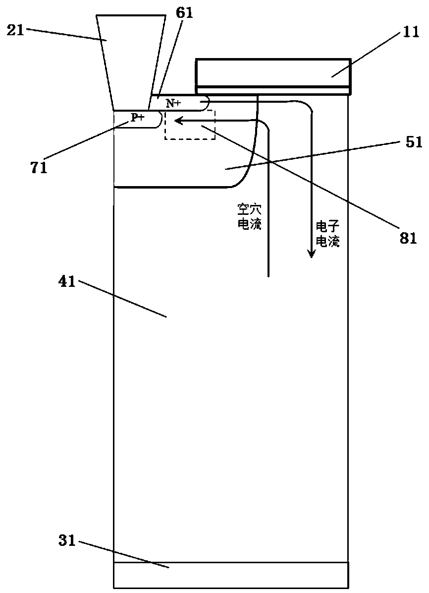
[0021] The structure of the gate-controlled power device in the prior art is as follows figure 1 As shown, it includes an N-type substrate 41 , a gate 11 , an emitter contact hole 21 , a collector 31 , a P-type well 51 , a heavily doped N-type region 61 and a heavily doped P-type region 71 . The region between the heavily doped P-type region 71 and the gate 11 is a region 81 .

[0022] During the processing of gate-controlled power devices in the prior art, hole current flows under the heavily doped N-type region 61 and is absorbed by the emitter. Since the emitter and the heavily doped N-type region 61 are always at zero potential, there will be doping in the P-type region (the P-type region includes the P-type well 51 and the heavily doped P-type region 71) below the heavily doped N-type region 61. As a result, there is a potential difference between the heavily doped N-type region 61 and the P-type region. When the hole current increases, especially when the device is tur...


PUM


Abstract

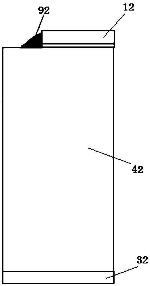
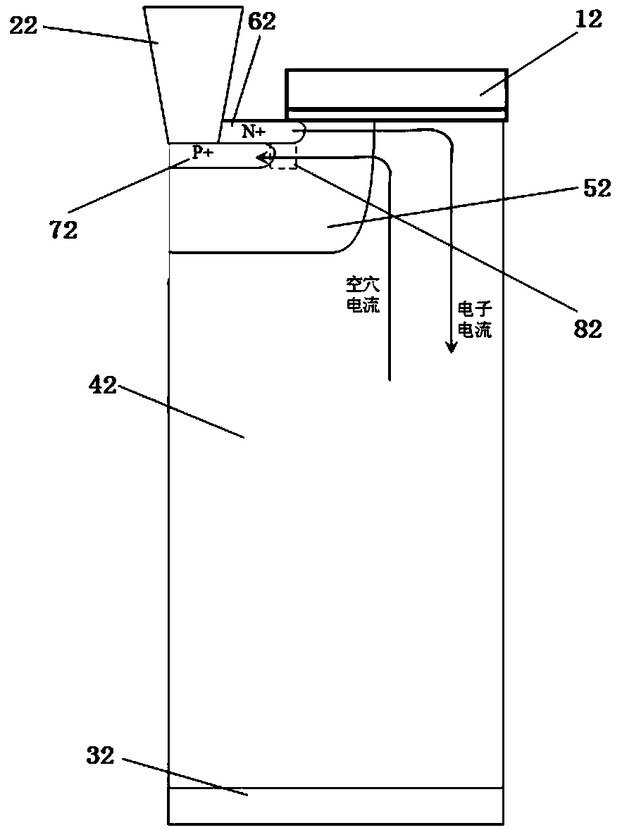
The invention discloses a self-alignment process for improving the performance of a safe working area of a gate-controlled power device. Before heavily doped P-type injection is carried out, a pad structure is formed in the direction of a gate end toward an emitter contact hole, and then the pad structure is used as a barrier for heavily doped P-type injection. After heavily doped P-type injectionis carried out, the pad structure is removed. According to the invention, the width of the pad structure can be adjusted by adjusting process parameters such as deposition time of a nitride layer, gas flow rate and pressure, so as to shorten the distance between a heavily doped P-type area and a gate to within 1 micron; the performance of the safe working area of the gate-controlled power deviceis greatly improved; the pad structure is used as the barrier; self-alignment of heavily doped P-type injection can be realized without the barrier of a photoresist; the influence of the deviation ofphotolithography process alignment between the emitter contact hole and the gate on the device is fundamentally eliminated; and the process provided by the invention is simple, and is conductive to improving the performance consistency of the device.

Description

technical field [0001] The invention relates to a grid-controlled power device, in particular to a self-alignment process for improving the performance of the safe working area of ​​the grid-controlled power device. Background technique [0002] Gate-controlled power devices (such as power MOSFETs and IGBTs) are modern and general-purpose power semiconductor devices, mainly used in new energy, locomotive traction, smart grid, high-voltage inverters and other fields. The energy-saving effect can reach 10%-40% by converting and controlling electric energy through power semiconductor devices. In the context of global warming, gate-controlled power device application technology is recognized as one of the best comprehensive methods to achieve global energy efficiency and carbon dioxide emission reduction goals. [0003] During the processing of gate-controlled power devices in the prior art, hole current flows under the heavily doped N-type region and is absorbed by the emitter...

Claims


Application Information

Patent Timeline
IPC IPC(8): H01L29/78H01L29/739H01L21/336H01L21/331
CPCH01L29/66325H01L29/66477H01L29/66537H01L29/7393H01L29/78
Inventor 刘剑郑泽人龚大卫王玉林
Owner YANGZHOU GUOYANG ELECTRONICS CO LTD
Learn More