Light-emitting device using quantum dot color conversion and its manufacturing method

A technology of light-emitting devices and quantum dot materials, applied in semiconductor devices, electrical components, circuits, etc., to achieve the effects of reducing oxidation, low water vapor permeability, and reducing the intensity of blue light per unit area

Active Publication Date: 2020-08-11
MAVEN OPTRONICS CO LTD
View PDF3 Cites 0 Cited by
  • Summary
  • Abstract
  • Description
  • Claims
  • Application Information

AI Technical Summary

Problems solved by technology

However, not all quantum dot materials are compatible with all adhesive materials. Usually, it is necessary to modify the surface of quantum dot materials first, such as forming ligands (Ligand), in order to uniformly disperse quantum dots in specific adhesive materials; therefore, the surface Modification, selection of specific adhesive materials, and process compatibility between different adhesive materials have also become important technical challenges for realizing the application of quantum dot materials in LED light-emitting devices

Method used


Image

  • Light-emitting device using quantum dot color conversion and its manufacturing method
  • Light-emitting device using quantum dot color conversion and its manufacturing method
  • Light-emitting device using quantum dot color conversion and its manufacturing method

Examples


Embodiment Construction

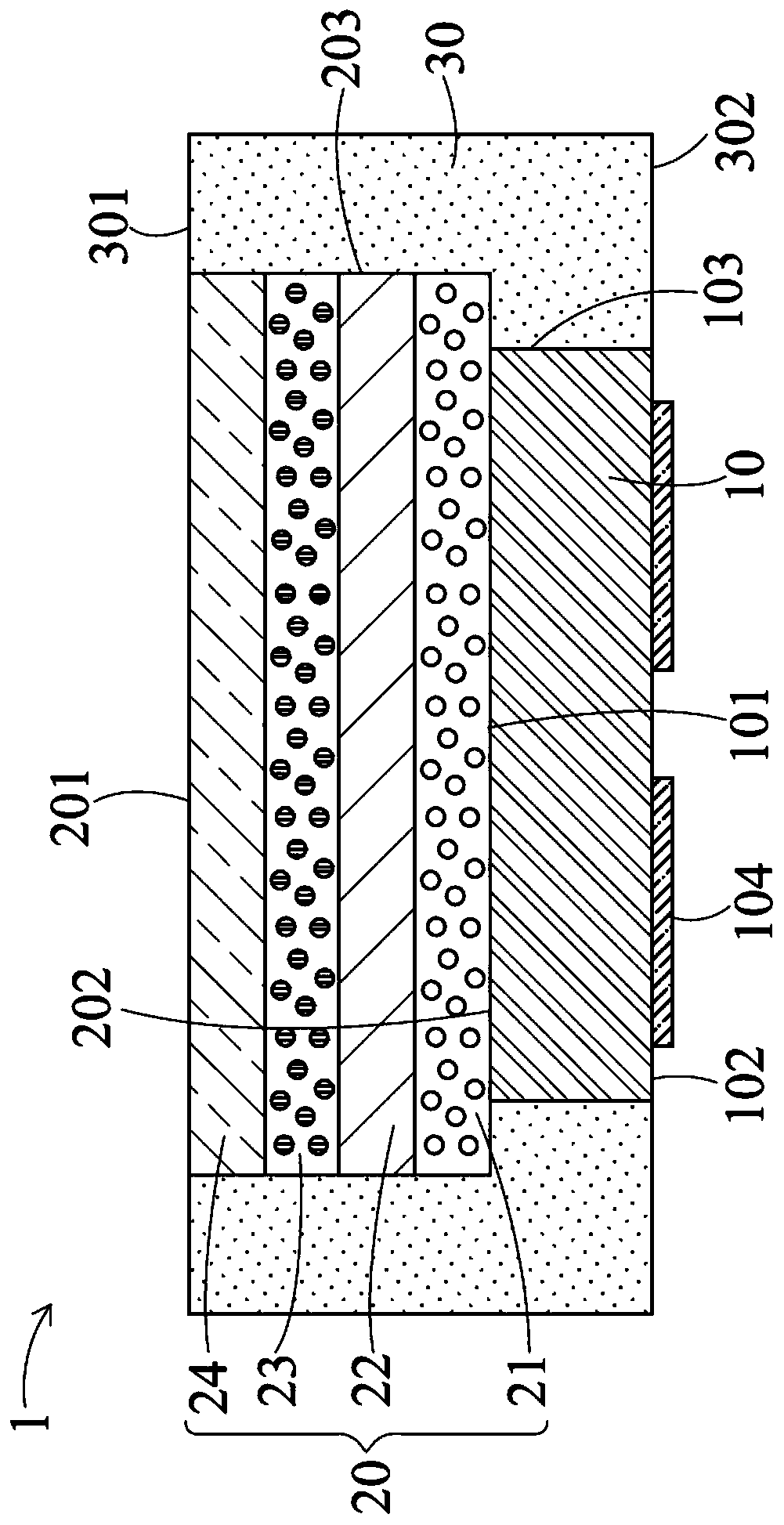
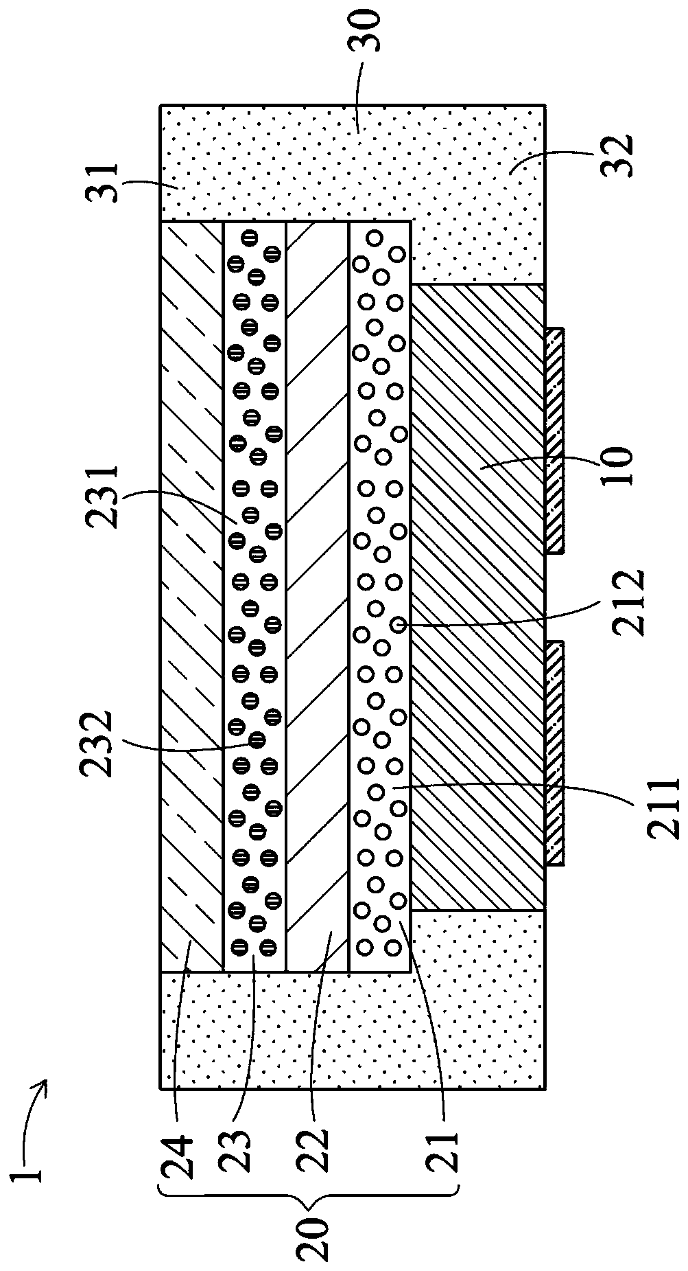
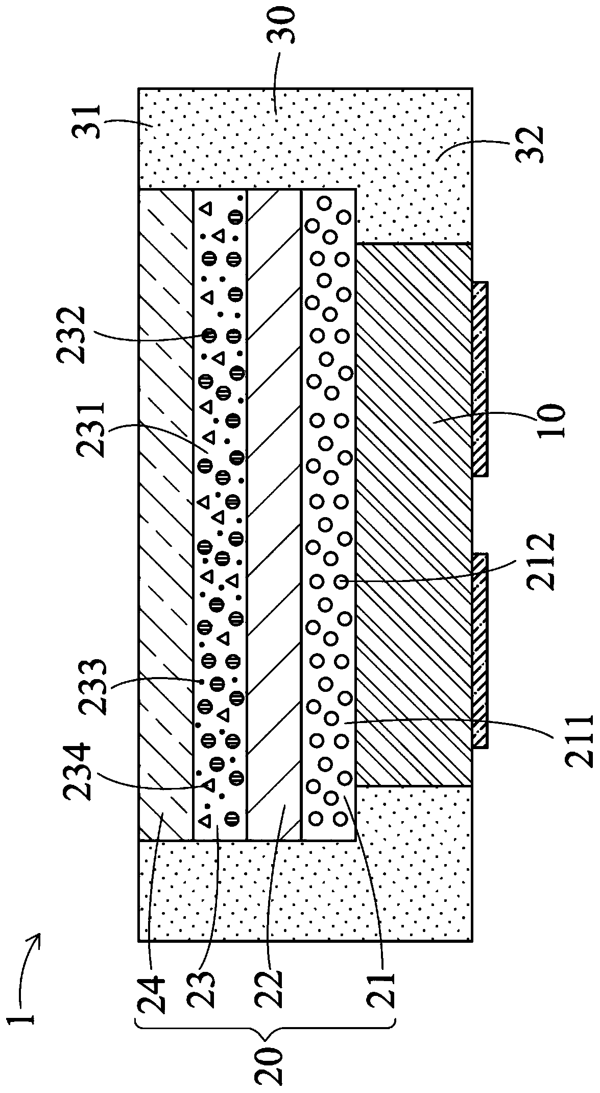
[0067] see Figure 1A and Figure 1B , which is a schematic diagram of the light emitting device 1 according to the first preferred embodiment of the present invention. The light emitting device 1 may include a flip-chip LED chip 10 , a photoluminescent structure 20 and a moisture barrier reflective structure 30 , and the technical content of each component will be described in sequence as follows.

[0068] The flip-chip LED chip (hereinafter referred to as the LED chip) 10 is used to provide a first light (or main light), which can be a blue light, a deep blue light, a purple light or a ultraviolet light and other higher energy level light; Taking a blue LED chip as an example, the first light provided by the LED chip 10 is blue light. The chip 10 may include an upper surface 101, a lower surface 102, a vertical surface 103 and an electrode group 104. The upper surface 101 and the lower surface 102 are oppositely arranged, and the vertical surface 103 is formed between the u...


PUM

PropertyMeasurementUnit
transmittivityaaaaaaaaaa

Abstract

The invention provides a light emitting device, which comprises a flip chip-type LED chip, a photo-luminescence structure and a moisture barrier reflection structure, wherein the photo-luminescence structure is arranged on the LED chip; the moisture barrier reflection structure covers the side surface of the photo-luminescence structure and the facade of the LED chip; and the photo-luminescence structure comprises a first photo-luminescence layer, a phototransparent isolation layer, a second photo-luminescence layer and a phototransparent moisture barrier layer sequentially stacked. In a better embodiment, the LED chip emits blue light, the first photo-luminescence layer contains a red fluorescent material and the second photo-luminescence layer contains green quantum dots, and thus, the red fluorescent material of the first photo-luminescence layer can firstly convert the higher-energy level blue light part to lower-energy level red light, the intensity of the non-converted blue lightirradiated on the green quantum dots is reduced, and photo-oxidation of the quantum dots can be effectively avoided. The invention also provides a manufacturing method for the above light emitting device.

Description

technical field [0001] The present invention relates to a chip-level packaging light-emitting device and a manufacturing method thereof, in particular to a chip-level packaging light-emitting device using green quantum dot materials and red fluorescent powder and a manufacturing method thereof. Background technique [0002] Quantum dot (quantum dot, QD) material is a semiconductor crystal material with a size of nanometer scale. Its particle size is usually between 1 nm and 50 nm. , the quantum dot material can convert part of the incident light into another lower energy level visible light, so the quantum dot material can be used as a photoluminescence material. By changing the particle size, shape or material composition of the quantum dot material, the quantum dot material can emit visible light of different wavelengths, that is, change its luminous spectrum. [0003] Compared with traditional fluorescent materials, such as yttrium aluminum garnet (YAG) phosphor, nitride...

Claims


Application Information

Patent Timeline
Patent Type & Authority Patents(China)
IPC IPC(8): H01L33/50H01L33/52H01L33/60
CPCH01L33/504H01L33/505H01L33/507H01L33/52H01L33/60H01L2933/0041H01L2933/005H01L2933/0058
Inventor 陈杰
Owner MAVEN OPTRONICS CO LTD
Why Eureka
Try Eureka