OLED structure, preparation method thereof, display panel and electronic device

An electrode and electrical connection technology, applied in circuits, electrical components, electrical solid devices, etc., can solve the problem of poor display effect on the display screen, achieve excellent display performance, reduce the probability of bulging or cracking, and ensure the effect of normal work

Active Publication Date: 2019-03-26
YUNGU GUAN TECH CO LTD
View PDF7 Cites 7 Cited by
  • Summary
  • Abstract
  • Description
  • Claims
  • Application Information

AI Technical Summary

Problems solved by technology

[0004] However, the display screens manufactured with flexible OLED technology in the prior art have the problem of poor display effect

Method used


Image

  • OLED structure, preparation method thereof, display panel and electronic device
  • OLED structure, preparation method thereof, display panel and electronic device
  • OLED structure, preparation method thereof, display panel and electronic device

Examples


Embodiment Construction

[0026] It can be seen from the background art that the display screen in the prior art has the problem of poor display effect.

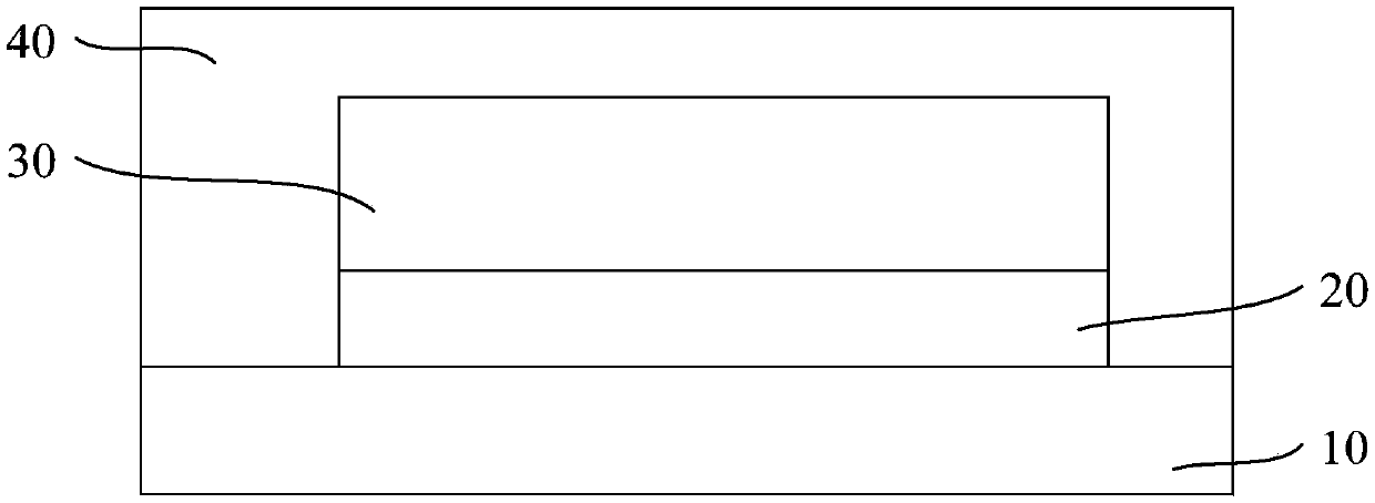
[0027] refer to figure 1 , figure 1 It is a schematic diagram of a partial cross-sectional structure of an existing OLED display screen, and the OLED display screen includes: a thin film transistor (TFT, Thin Film Transistor) 10; a multilayer structure 20 located on the thin film transistor 10, the multilayer structure 20 includes an anode layer and An organic functional layer on the surface of the anode layer; a cathode layer 30 on the surface of the multilayer structure 20; an encapsulation layer 40 covering the cathode layer 30, the surface of the TFT 10 and the sidewall of the multilayer structure 20.

[0028] The inventors have found that during the dynamic bending process of the OLED display, the film layer is easily damaged in the bending area, which will lead to poor display effect or even display failure. The main reason is that the thin f...


PUM


Abstract

The present invention provides an OLED structure, a preparation method thereof, a display panel and an electronic device. The OLED structure includes an array substrate, a first electrode on one sideof the array substrate, a plurality of light emitting units, a pixel defining layer separating the light emitting units, and a second electrode arranged opposite to the first electrode. The pluralityof light emitting units are corresponding to light emitting regions of the OLED structure, and the pixel defining layer is corresponding to a non-light-emitting region of the OLED structure. The OLEDstructure further comprises an auxiliary electrode which is located in the non-light-emitting region and is electrically connected to the first electrode and / or the second electrode, and the materialof the auxiliary electrode is a conductive fiber material. The auxiliary electrode has good electrical conductivity and bending resistance, the circuit is damaged when the first electrode or the second electrode is broken is prevented, and the reliability of the electrodes of the OLED structure is improved.

Description

technical field [0001] The embodiments of the present invention relate to the field of display, and in particular to an OLED structure and a manufacturing method thereof, a display panel and electronic equipment. Background technique [0002] OLED (Organic Light-Emitting Diode) is called an organic light-emitting diode. OLED display technology has many advantages such as full solid state, active light emission, high contrast, ultra-thin, low power consumption, fast effect speed, wide working range, easy realization of flexible display and 3D display, etc., making it widely used in many display devices at present. , for example on televisions and mobile devices. [0003] Flexible OLED refers to a flexible organic light emitting diode, which is manufactured based on a flexible substrate and operates on the flexible substrate. Compared with traditional rigid OLEDs, flexible OLEDs are more flexible, lighter and thinner, making foldable and rollable display technologies possibl...

Claims


Application Information

Patent Timeline
Patent Type & Authority Applications(China)
IPC IPC(8): H01L27/32H01L51/52H01L51/56B82Y40/00
CPCB82Y40/00H10K59/131H10K50/822H10K50/824H10K59/1201H10K71/00
Inventor 吕磊刘胜芳董晴晴张义波张浩杰
Owner YUNGU GUAN TECH CO LTD
Why Eureka
Try Eureka