A Gan-based High Voltage Rectifier Resonant Tunneling Diode

A resonant tunneling and high-voltage rectification technology, which is applied in the direction of diodes, semiconductor devices, electrical components, etc., can solve the problems of difficult process compatibility, GaN-based integrated devices and ESD protection of integrated circuits, so as to avoid difficulties and troubles and have good compatibility Effect

Active Publication Date: 2022-03-29
SHANGRAO NORMAL UNIV
View PDF9 Cites 0 Cited by
  • Summary
  • Abstract
  • Description
  • Claims
  • Application Information

AI Technical Summary

Problems solved by technology

[0012] The core protection devices used in the above ESD protection schemes are all silicon-based devices. Although they are widely used in the ESD protection of silicon-based integrated devices and circuits, they are difficult to be directly used in the ESD protection of GaN-based integrated devices and integrated circuits due to process compatibility issues.

Method used


Image

  • A Gan-based High Voltage Rectifier Resonant Tunneling Diode
  • A Gan-based High Voltage Rectifier Resonant Tunneling Diode
  • A Gan-based High Voltage Rectifier Resonant Tunneling Diode

Examples


Embodiment Construction

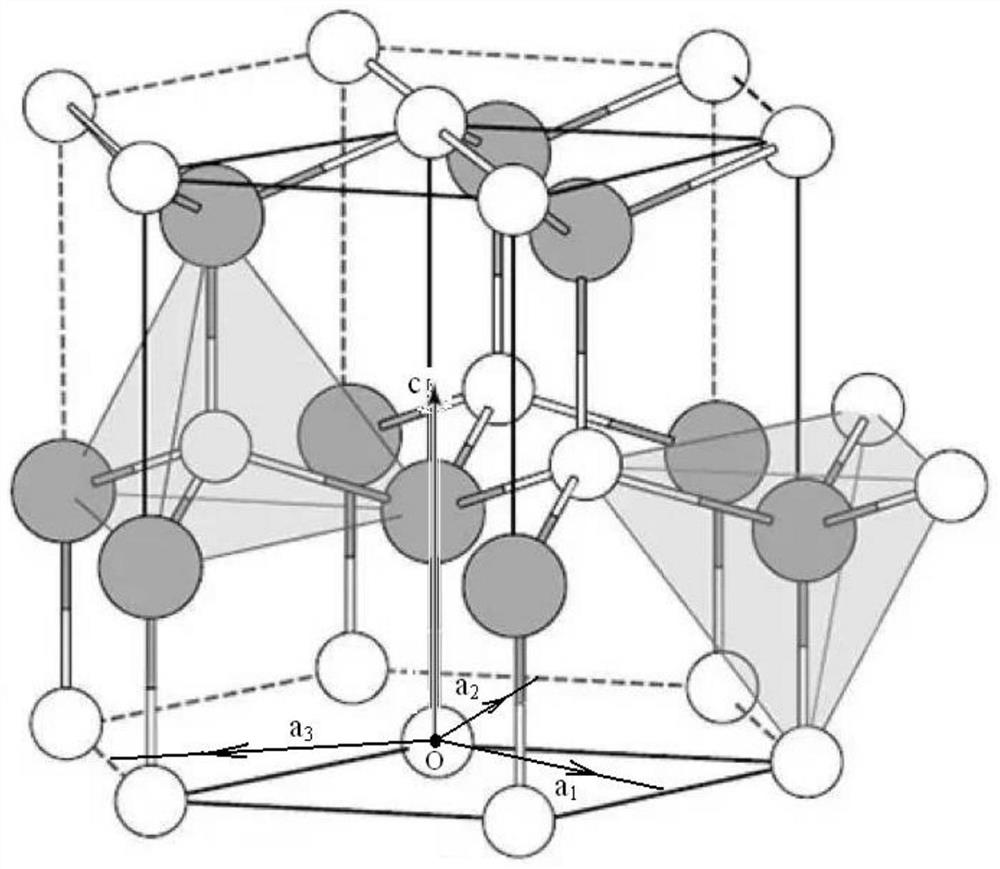
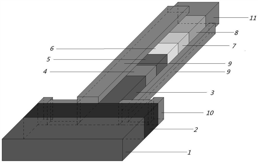
[0037] as attached figure 2 shows a GaN-based high-voltage rectifier resonant tunneling diode (HVRRTD), including i-GaN semi-insulating substrate 1, n + -In 0.07 Ga 0.93 N collector layer 2, i-In 0.07 Ga 0.93 N first isolation layer 3, i-Al 0.1 Ga 0.9 N first barrier layer 4, i-In 0.14 Ga 0.86 N quantum well layer 5, i-GaN second barrier layer 6, i-In 0.21 Ga 0.79 N second isolation layer 7, n + -In 0.21 Ga 0.79 N emitter layer 8, AlN, Si 3 N 4 or SiO 2The passivation layer 9, the metal electrode pins 10 in the collector area and the metal electrode pins 11 in the emitter area. The upper surface of the i-GaN substrate 1 with a thickness of 300-500 μm is epitaxially extended to a thickness of 0.1-0.5 μm + -In 0.07 Ga 0.93 N collector layer 2, epitaxial 24-60nm thick i-In in the middle of the upper surface of collector layer 2 0.07 Ga 0.93 N first isolation layer 3, 1.5-6nm thick i-Al 0.1 Ga 0.9 N first barrier layer 4, 1.5-3nm thick i-In 0.14 Ga 0.86 N q...


PUM

PropertyMeasurementUnit
thicknessaaaaaaaaaa

Abstract

The invention relates to a GaN-based high-voltage rectification resonant tunneling diode. The present invention includes planar GaN substrates, n + -In 0.07 Ga 0.93 N collector layer, i‑In 0.07 Ga 0.93 N first spacer layer, AlGaN first barrier layer, i‑In 0.14 Ga 0.86 N quantum well layer, GaN second barrier layer, i‑In 0.21 Ga 0.89 N second isolation layer, n + -In 0.21 Ga 0.89 N emitter layer, passivation layer, collector metal electrode pins and emitter metal electrode pins. This kind of GaN-based high-voltage resonant tunneling diode—HVRTD has volt-ampere characteristics of high forward blocking voltage and reverse ultra-low resistivity, and its manufacturing process is compatible with GaN-based integrated devices and circuits (including circuits, optical circuits, magnetic circuits, It is compatible with the micro-nano integrated manufacturing process of gas circuit, mechanical circuit and composite circuit, and is very suitable for ESD protection applications of GaN-based integrated devices and circuits. It can withstand ±2000V ESD within an approximately ideal time of 840ns to ensure GaN-based integrated devices and The road is not damaged.

Description

technical field [0001] The invention relates to the technical field of compound semiconductor quantum devices, in particular to a GaN-based high-voltage rectifying resonant tunneling diode (HVRRTD). Background technique [0002] For conventional GaN / AlGaN resonant tunneling diode (RTD) devices, due to the significant spontaneous polarization effect of the GaN / AlGaN barrier layer and the significant piezoelectric polarization effect under the action of an applied voltage, the GaN / AlGaN barrier layer will form polarized electric field. Due to the constraints of the intrinsic structure of GaN / AlGaN materials and the kinetics of epitaxial growth on the surface, for the c-plane epitaxial growth, the epitaxial growth of high-quality GaN / AlGaN nanofilms has the same initial polar plane as the final polar plane. If the upper surface of the GaN substrate is c-plane, that is, the polarity of the Ga surface, the direction of the polarization electric field in the AlGaN barrier layer i...

Claims


Application Information

Patent Timeline
Patent Type & Authority Patents(China)
IPC IPC(8): H01L29/06H01L29/88
CPCH01L29/0611H01L29/0646H01L29/882
Inventor 张海鹏耿露王晓媛张忠海林弥陆雪杰
Owner SHANGRAO NORMAL UNIV
Why Eureka
Try Eureka