
4h-sic metal-semiconductor field-effect transistor with lightly doped gate edge and drain side parts

A field-effect transistor and metal-semiconductor technology, which is applied in the field of 4H-SiC metal-semiconductor field-effect transistors, can solve problems such as life-span impact, limited device working environment and reliability, and easy breakdown of devices, so as to improve lifespan and relieve heat. Electron charging effect, hot carrier reduction effect

Active Publication Date: 2021-06-25
XIDIAN UNIV
View PDF3 Cites 0 Cited by
  • Summary
  • Abstract
  • Description
  • Claims
  • Application Information

AI Technical Summary

Problems solved by technology

However, the electric field concentration effect and hot electron charging effect on the drain side of the gate edge have not been effectively improved, which makes the device easy to be broken down, and the life is greatly affected, which limits the working environment and reliability of the device

Method used


Image

  • 4h-sic metal-semiconductor field-effect transistor with lightly doped gate edge and drain side parts

Examples


Embodiment 1

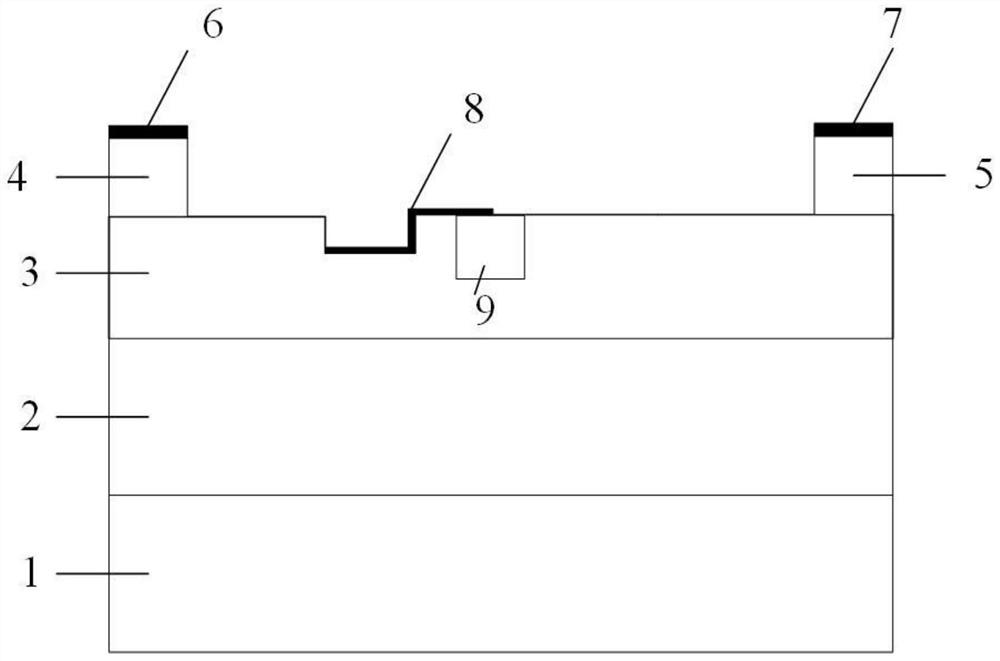
[0018] Such as figure 1 As shown, the 4H-SiC metal-semiconductor field-effect transistor with lightly doped gate edge and drain side parts provided in this embodiment includes a 4H-SiC semi-insulating substrate 1, a P-type buffer layer 2, and an N-type channel from bottom to top. Channel layer 3, the upper surface of the N-type channel layer 3 is provided with a source cap layer 4 and a drain cap layer 5, the upper surface of the source cap layer 4 is provided with a source electrode 6, and on the drain cap layer 5 A drain electrode 7 is provided on the surface, a gate electrode 8 is provided at the bottom of the N-type channel layer 3 and on the side close to the source cap layer 4, and a gate electrode 8 is provided at the bottom of the N-type channel layer 3 and is located under the gate of a part of the gate electrode 8 and part of the gate A lightly doped region 9 is formed between the drains, and the lightly doped region 9 has an axisymmetric structure taking the vertica...


PUM

PropertyMeasurementUnit
depthaaaaaaaaaa
lengthaaaaaaaaaa
lengthaaaaaaaaaa

Abstract

The invention discloses a 4H-SiC metal-semiconductor field effect transistor with light doping on the drain side of the gate edge, including a 4H-SiC semi-insulating substrate, a P-type buffer layer, an N-type channel layer, and an N-type channel from bottom to top. Both sides of the upper surface of the channel layer are provided with a source cap layer and a drain cap layer, the upper surface of the source cap layer is provided with a source electrode, the upper surface of the drain cap layer is provided with a drain electrode, and the bottom of the N-type channel layer is close to the source One side of the pole cap layer is provided with a gate electrode, and a lightly doped region is formed at the bottom of the N-type channel layer under the gate of a part of the gate electrode and between part of the gate and drain. The vertical line is the axis of symmetry and the structure is axisymmetric. The invention can alleviate the electric field concentration effect on the drain side of the gate edge to optimize the electric field and current on the drain side of the gate edge, thereby suppressing breakdown; it can alleviate the hot electron charging effect, so as to reduce the generation of interface states and suppress the decline of device performance, thereby Improve device life.

Description

technical field [0001] The invention relates to the technical field of field effect transistors, in particular to a 4H-SiC metal-semiconductor field effect transistor with light doping on the drain side of the gate edge. Background technique [0002] SiC materials have outstanding material and electrical properties such as wide band gap, high breakdown electric field, high saturated electron migration velocity, and high thermal conductivity, making them suitable for high-frequency and high-power device applications, especially high temperature, high voltage, aerospace, satellite, etc. It has great potential in high-frequency high-power device applications in harsh environments. In SiC allomorphs, the electron mobility of 4H-SiC with hexagonal close-packed wurtzite structure is nearly three times that of 6H-SiC, so 4H-SiC materials are used in high-frequency and high-power devices, especially in metal-semiconductor fields. Effect transistor (MESFET) occupies a major position...

Claims


Application Information

Patent Timeline
Patent Type & Authority Patents(China)
IPC IPC(8): H01L29/786H01L29/06H01L29/10
CPCH01L29/0619H01L29/0684H01L29/1041H01L29/78681
Inventor 贾护军李涛仝宜波朱顺威胡梅赵玥阳杨银堂
Owner XIDIAN UNIV
Learn More