Immersive surface plasmon interference lithography method with adjustable resolution

A surface plasmon, interference lithography technology, applied in the field of micro-nano structure processing, can solve problems such as unfavorable photoresist exposure

Inactive Publication Date: 2019-03-29
GUANGXI UNIV
View PDF2 Cites 2 Cited by
  • Summary
  • Abstract
  • Description
  • Claims
  • Application Information

AI Technical Summary

Problems solved by technology

However, the current surface plasmon interference lithography methods using gratings as masks all have the problem that the mask and photoresi

Method used


Image

  • Immersive surface plasmon interference lithography method with adjustable resolution
  • Immersive surface plasmon interference lithography method with adjustable resolution
  • Immersive surface plasmon interference lithography method with adjustable resolution

Examples


Embodiment 1

[0037] Example 1, making a nanowire array pattern with a line width of 21nm and a period of 42nm.

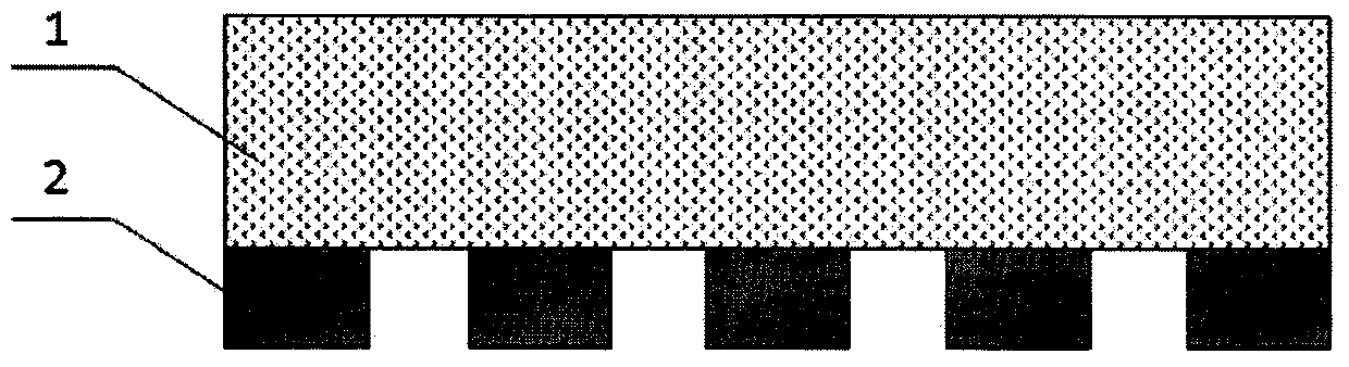
[0038] 1) Coating an aluminum film with a thickness of 40nm on the surface of the quartz glass plate by magnetron sputtering, and then using focused ion beam lithography to produce a grating with a line width of 50nm and a period of 84nm to complete the production of the aluminum mask, as figure 1 shown;

[0039] 2) Spin-coat a layer of polymethacrylate (PMMA) with a thickness of 15nm on the aluminum mask;

[0040] 3) leave the PMMA in the step 2) until it solidifies completely;

[0041] 4) Coating a layer of MgF with a thickness of 15nm by magnetron sputtering on the surface of PMMA 2 Thin film as additional medium film;

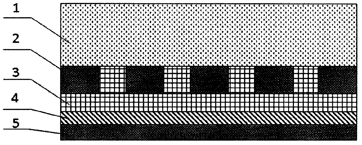
[0042] 5) On the surface of the additional dielectric film, magnetron sputtering is used to plate an aluminum film with a thickness of 20nm as an additional aluminum film to obtain an aluminum mask structure with an additional film, such as figure 2 show...

Embodiment 2

[0049] Example 2, making a nanowire array pattern with a line width of 16nm and a period of 32nm.

[0050]1) Coating an aluminum film with a thickness of 30nm on the surface of a quartz glass plate by magnetron sputtering, and then using focused ion beam lithography to produce a grating with a line width of 30nm and a period of 64nm to complete the production of an aluminum mask, as figure 1 shown;

[0051] 2) Spin-coat a layer of polymethacrylate (PMMA) with a thickness of 15nm on the aluminum mask;

[0052] 3) leave the PMMA in the step 2) until it solidifies completely;

[0053] 4) Coating a layer of SiO with a thickness of 10 nm on the surface of PMMA by magnetron sputtering 2 Thin film as additional medium film;

[0054] 5) On the surface of the additional dielectric film, magnetron sputtering is used to plate an aluminum film with a thickness of 15nm as an additional aluminum film to obtain an aluminum mask structure with an additional film, such as figure 2 shown; ...


PUM

PropertyMeasurementUnit
Thicknessaaaaaaaaaa
Thicknessaaaaaaaaaa
Thicknessaaaaaaaaaa

Abstract

The invention discloses an immersive surface plasmon interference lithography method with adjustable resolution. The method comprises steps of (1) preparing an aluminum mask plate on the surface of aglass plate; (2) spin coating the aluminum mask plate with a layer of polymethyl methacrylate (PMMA); (3) placing stilly the PMMA in the step (2) until the PMMA is fully solidified; (4) plating the surface of the PMMA with an additional dielectric film; (5) plating the surface of the additional dielectric film with an additional aluminum film; (6) plating a photoresist substrate with an aluminum film; (7) spin coating the surface of the aluminum film on the photoresist substrate with a layer of photoresist; (8) dripping an immersive liquid onto the surface of the photoresist; (9) placing the aluminum mask plate with the additional film over the surface of the photoresist and connecting the additional aluminum film of the aluminum mask plate to the photoresist by the immersive liquid; (10)vertically illuminating the mask plate with monochromatic parallel light to complete the exposure; (11) developing the photoresist to obtain a lithographic pattern . The method can produce nanowire arrays or gratings with different periods under the condition that the illumination wavelength is constant, and can conveniently produce nanowire arrays or gratings on different substrates in large batches and efficiently due to the use of the immersive liquid.

Description

technical field [0001] The invention belongs to the technical field of micro-nano structure processing, and in particular relates to a surface plasmon interference photolithography method. Background technique [0002] Photolithography is one of the commonly used techniques for processing micro-nanostructures. Due to the advantages of low cost and high efficiency, photolithography technology has been widely used in the fields of processing electronic chips and integrated optical devices. However, traditional lithography technology is limited by the diffraction limit of light, and it is difficult to continue to improve the resolution of lithography. This limits the application of traditional photolithography in many fields. [0003] Surface plasmons are surface electromagnetic waves that exist at the interface between a metal and a medium. Since its wavelength is much smaller than that of illumination light, its application in lithography can improve the resolution of lith...

Claims


Application Information

Patent Timeline
IPC IPC(8): G03F7/20G02B5/00
CPCG02B5/008G03F7/70033G03F7/70341G03F7/70408
Inventor 董建杰张卫平
Owner GUANGXI UNIV
Why Eureka
Try Eureka