Electric field analysis method of electromagnetic pulse nano-semiconductor device

A nano-semiconductor and electromagnetic pulse technology, applied in the field of electric field analysis, can solve problems such as huge amount of calculation and waste of time, and achieve the effect of flexible modeling, less unknowns, and saving computing time.

Active Publication Date: 2019-03-29
NANJING UNIV OF SCI & TECH
View PDF1 Cites 1 Cited by
  • Summary
  • Abstract
  • Description
  • Claims
  • Application Information

AI Technical Summary

Problems solved by technology

Considering that the electrical parameters in the electromagnetic pulse are time-varying functions, it is more appropriate to use the time-domain method. Generally, FDTD and FEM are more commonly used. However, due to the Yee grid characteristics of FDTD, it is easy to be limited when simulating a model with a complex structure. The application of FEM In the time domain, each time step involves the solution of linear equations, the amount of calculation is very large, and it is a waste of time

Method used


Image

  • Electric field analysis method of electromagnetic pulse nano-semiconductor device
  • Electric field analysis method of electromagnetic pulse nano-semiconductor device
  • Electric field analysis method of electromagnetic pulse nano-semiconductor device

Examples


Embodiment Construction

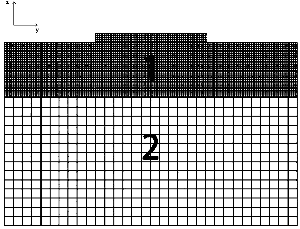
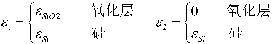
[0042] The present invention is an electric field analysis method of a nanometer semiconductor device under the action of an electromagnetic pulse. The method adopts the time-domain spectral element method to solve the density gradient equation group. The density gradient equation group is a nonlinear equation group, so the discontinuous Galerkin time-domain spectrum is used. The elemental method calculates the instantaneous carrier concentration, potential distribution and carrier Fermi potential of semiconductor devices under the action of electromagnetic pulse and voltage, and obtains the electric field strength and current density at the current moment. This analysis method is based on the MOSFET physical model. Under the same electromagnetic pulse and voltage, the field change in the channel region is more severe, and the field change in the substrate region is relatively flat. Therefore, discontinuous meshing can be carried out, and the channel region can be The fine grid...


PUM


Abstract

The invention discloses an electric field analysis method of an electromagnetic pulse nano semiconductor device. The steps of the method are as follows: in the first step, the solution model of MOSFETis established, and the model is divided by using the curved hexahedrons to obtain the structural information of the model, including the element information and node information of the hexahedron; in the second step, starting from the carrier current continuity equation, Poisson equation and carrier quantum correction equation, the backward Euler time difference is used firstly, then the discontinuous Galerkin method is used to test the equation, and the electric field boundary condition is imposed to obtain the electric field and current distribution of each node. On the premise of the samecalculation amount, Under the action of electromagnetic pulse and voltage, the distribution of the internal electric field with time can be obtained more clearly, which can reduce the computational load when the convergence accuracy is the same. In addition, the method has the advantages of flexible modeling and convenient dissection, and the formed matrix has good sparsity and high efficiency ofsolution.

Description

technical field [0001] The invention belongs to the technical field of electric field analysis, in particular to an electric field analysis method for electromagnetic pulse nanometer semiconductor devices. Background technique [0002] An electromagnetic pulse is a transient electromagnetic phenomenon. After the high-power electromagnetic pulse is injected into the integrated circuit, it will cause the electrical breakdown of the circuit, and even completely damage the device. Integrated circuits and electronic equipment are mainly composed of semiconductor devices. As the integration level of circuits continues to increase, they are becoming more and more sensitive to strong electromagnetic pulses, especially high-power electromagnetic pulses. Active components in circuits, especially MOSFETs, easily absorb radiated electromagnetic energy and are prone to Affected by electrical stress, it will fail or even be damaged. In order to take effective measures to protect electro...

Claims


Application Information

Patent Timeline
Patent Type & Authority Applications(China)
IPC IPC(8): G06F17/50
CPCG06F30/20Y02E60/00
Inventor 何云峰丁大志姚猛籍宇豪陈如山
Owner NANJING UNIV OF SCI & TECH
Why Eureka
Try Eureka