
Nonlinear transmission line comb wave generating circuit

A technology of nonlinear transmission line and generating circuit, applied in the field of signal source, can solve the problems of low cost, complicated circuit debugging, cumbersome circuit structure, etc., and achieve the effect of low cost

Pending Publication Date: 2019-04-02
CHINA ELECTRONIS TECH INSTR CO LTD
View PDF3 Cites 0 Cited by
  • Summary
  • Abstract
  • Description
  • Claims
  • Application Information

AI Technical Summary

Problems solved by technology

The big disadvantage of these two methods is that the circuit debugging is complicated. The step tube in the first method is a highly nonlinear component, which is easy to cause self-excitation and oscillation of the circuit, so it needs to be carefully debugged in actual work.
In the second method, transistors working in the avalanche region are prone to avalanche oscillation, and can only work at lower frequencies, so the application range is limited
At present, NLTLs chips are basically foreign products, and the price is very expensive.
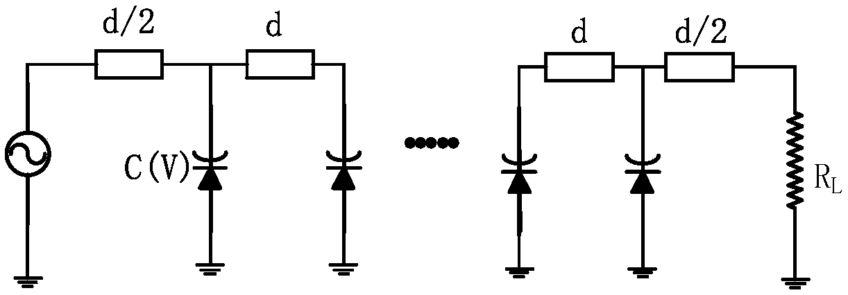
If the comb wave effect of NLTLs can be simulated on the board level, it will have a huge market prospect. The existing technical solutions are realized by using Schottky diodes like chips. The solutions are as follows: figure 1 As shown, d in the scheme is a microstrip line, and the diode is a Schottky diode. In the scheme, the cascade connection of nearly 20 knots, the effect of edge compression is not very good, and it is difficult to meet the current market application. The reason is very To achieve a certain edge compression effect and achieve rich harmonic components, a linear transmission line often requires a relatively large number of cascades, often more than 50 cascades, and it is difficult to achieve so many levels at the board level due to limited space. Cascaded, although so many stages are really cascaded, due to the relatively large resistance dissipation at the board level, the harmonic components will also be exhausted, which will not have a good effect
[0006] 1. The traditional method of frequency synthesis, that is, the method of multiple frequency multiplication, frequency division and frequency mixing, has a complicated circuit structure, occupies a large area, and is easy to introduce stray and additional noise. Due to the use of many devices, the cost is low Not low
[0007] 2. The highest frequency of SRD comb wave generation technology can only reach 18GHz, and due to its working mechanism, the phase noise of SRD is difficult to suppress very well, usually it is best to have about 3dB of additional noise, so in high-end instruments SRD technology is usually not used on
[0008] 3. The chips of nonlinear transmission lines (NLTLs) have good performance, but almost all of them are foreign products, the price is extremely high and most of them are embargoed. Considering the cost performance of the instrument and independent intellectual property rights, they are usually not used
[0009] 4. At present, the technical effect of using engineering methods to simulate the effect of NLTLs at the board level in China is not good. On the one hand, the cascading method of using more than 20 levels of Schottky diodes cannot be compared with dozens or even hundreds of levels of chips. Compared with the cascade effect, it is impossible to realize the technical indicators of 100MHz-1GHz signal input, 1GHz-10GHz output power above -20dBm, and frequency response within 15dB. It is too small to achieve the miniaturization goal of our high-end instruments

Method used


Image

  • Nonlinear transmission line comb wave generating circuit
  • Nonlinear transmission line comb wave generating circuit
  • Nonlinear transmission line comb wave generating circuit

Examples


Embodiment Construction

[0023] Below in conjunction with accompanying drawing and specific embodiment the present invention is described in further detail:

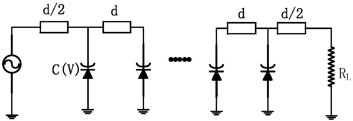
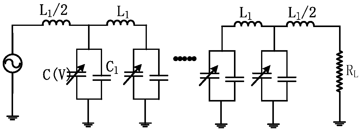
[0024] The non-linear transmission line microstrip circuit consists of figure 2 As shown, its approximate equivalent circuit model consists of series inductors and parallel capacitors, such as image 3 As shown, in general, the two circuits can be approximately equivalent.

[0025] According to the excitation line theory of nonlinear transmission line: when the voltage of the input signal is changed by V 1 change to V 2 When , the time when its waveform is compressed can be expressed as:

[0026]

[0027] Then the time when the rising or falling edge of the input signal is compressed after passing through the single-section network can be expressed as:

[0028]

[0029] Among them, L l and C l is the equivalent inductance and capacitance of the microstrip line, C(V) is the value of the capacitance changing with the voltage when the ...


PUM


Abstract

The invention discloses a nonlinear transmission line comb wave generating circuit, belonging to the field of signal sources. The nonlinear transmission line comb wave generating circuit comprises a power source, a reference generating circuit and a resistor, wherein the power source, the reference generating circuit and the resistor are connected by means of a line; the reference generating circuit comprises a plurality of inductors and a plurality of variable capacitance diodes; the inductors are connected in series; and the diodes are arranged in groups, each group consists of two diodes which are symmetrically distributed on both sides of one inductor, and the groups of diodes are distributed in parallel. Compared with the conventional frequency synthesizing circuit, the nonlinear transmission line comb wave generating circuit has the advantages of space reduction of 12% and cost reduction of 10%; compared with the SRD technology, the nonlinear transmission line comb wave generating circuit has better frequency response and phase noise properties; compared with an NLTL chip, the nonlinear transmission line comb wave generating circuit is low in cost, and is autonomous and controllable; and the nonlinear transmission line comb wave generating circuit requires fewer stages, saves more circuit space, and more importantly, has an edge compression effect far superior to that ofthe existing Schottky NLTL circuit, thereby the acquired frequency response and output power are more excellent.

Description

technical field [0001] The invention belongs to the field of signal sources, and in particular relates to a comb wave generating circuit of a nonlinear transmission line. Background technique [0002] The reference signal is the basis of the overall signal output of the signal source instrument, and directly determines the phase noise level of the overall signal. At present, high-performance signal generators all use multi-point reference signals with equal intervals of hundreds of megahertz. The generation method is still the traditional frequency synthesis method, that is, the method of multiple frequency multiplication, frequency division and frequency mixing. Its circuit The structure is cumbersome and occupies a large area, and it is easy to introduce stray and additional noise. In order to realize the miniaturization of the circuit, the reference generation circuit can adopt comb wave frequency multiplication technology based on nonlinear transmission line or SRD. The...

Claims


Application Information

Patent Timeline
Patent Type & Authority Applications(China)
IPC IPC(8): H03K3/57
CPCH03K3/57
Inventor 周帅刘亮刘青松卢凯范吉伟周玉勇
Owner CHINA ELECTRONIS TECH INSTR CO LTD
Learn More