A silicon-lithium niobate heterogeneous integrated scanning chip and its preparation method and application

A scanning chip, lithium niobate technology, applied in the direction of instruments, optical waveguide light guide, optics, etc., can solve the problems of heterogeneous integrated structure design, large waveguide transmission loss, low modulation efficiency, etc., and achieve high-speed phase shifting of beams Deflection, low transmission loss, compact structure effect

Active Publication Date: 2020-08-07
UNIV OF SHANGHAI FOR SCI & TECH
View PDF8 Cites 0 Cited by
  • Summary
  • Abstract
  • Description
  • Claims
  • Application Information

AI Technical Summary

Problems solved by technology

However, since the second-order nonlinear optical coefficient of the silicon material itself is very small, it is difficult to realize electro-optical modulation. Therefore, it is often necessary to modulate the optical properties of the material by changing the concentration of the external carrier, and then realize the modulation of light waves, such as forming p-i-n by ion implantation. type structure, but this also leads to a large transmission loss of the waveguide, and the modulation efficiency is not high
Therefore, for the heterogeneous integration of low-loss waveguides and lithium niobate materials, so far, there has not been a structural design for the heterogeneous integration of silicon waveguide substrates and lithium niobate materials for the 1520 nm to 1620 nm optical communication band. and ways to achieve

Method used


Image

  • A silicon-lithium niobate heterogeneous integrated scanning chip and its preparation method and application
  • A silicon-lithium niobate heterogeneous integrated scanning chip and its preparation method and application
  • A silicon-lithium niobate heterogeneous integrated scanning chip and its preparation method and application

Examples


Embodiment Construction

[0038] The silicon-lithium niobate heterogeneous integrated scanning chip of the present invention will be described in more detail below in conjunction with the schematic diagram, wherein a preferred embodiment of the present invention is represented, it should be understood that those skilled in the art can modify the present invention described here, and still The advantageous effects of the present invention are realized. Therefore, the following description should be understood as the broad knowledge of those skilled in the art, but not as a limitation of the present invention.

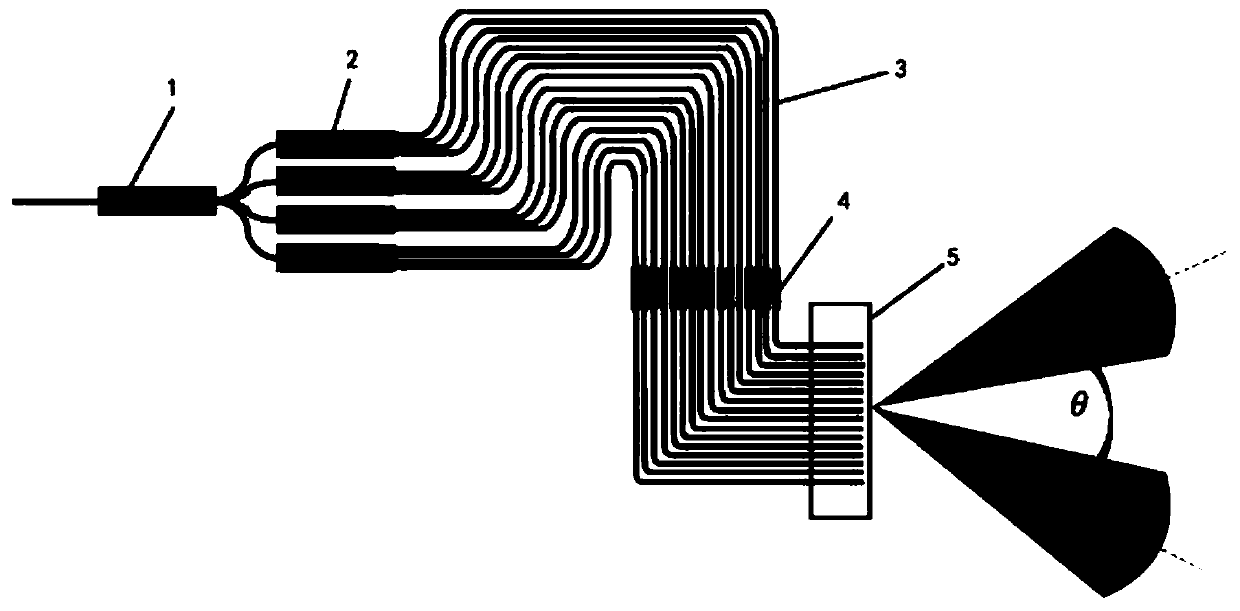
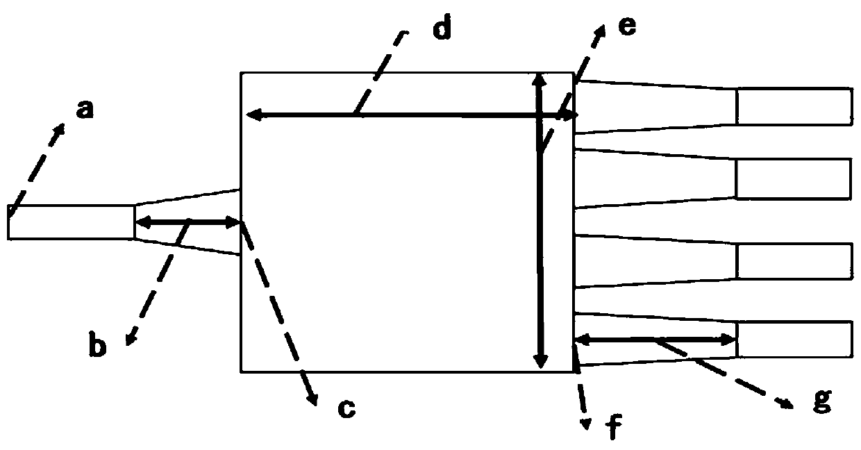
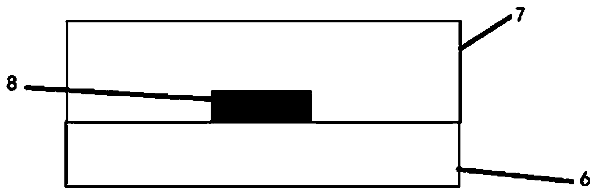
[0039] Such as figure 1 , image 3 As shown, a silicon-lithium niobate heterogeneous integrated scanning chip includes a lithium niobate substrate 6, a silicon dioxide cladding layer 7, and a silicon waveguide-based core layer 8; the silicon dioxide slow cladding layer 7 is attached to niobate On the lithium substrate 6; the core layer 8 includes an optical beam splitting unit, a curved wavegui...


PUM

PropertyMeasurementUnit
lengthaaaaaaaaaa
depthaaaaaaaaaa
widthaaaaaaaaaa

Abstract

The invention provides a silicon-lithium niobate heterogeneity integrated scanning chip. The chip comprises a lithium niobate substrate, a silica cladding layer, and a silicon waveguide based core layer. The silica cladding layer is attached to the lithium niobate substrate. The core layer comprises an optical beam splitting unit, a curved waveguide, a thermo-optical phase shifter, and an emergentwaveguide array. The optical beam splitting unit, the curved waveguide, and the emergent waveguide array are located in the silica cladding layer. The thermo-optical phase shifter is disposed on thesilica cladding layer and is located on the curved waveguide. The optical beam splitting unit comprises a plurality of silicon waveguide based beam splitters. According to the silicon-lithium niobateheterogeneity integrated scanning chip, the silicon waveguide substrate is integrated with the heterogeneity of the lithium niobate material, and thermo-optic modulation is used based on the optical phased array technology, so as to change the the refractive index of the waveguide, change the phase of the beam, and deflect the exit direction, thereby obtaining a high-speed low-loss optical modulation chip structure of 1520nm to 1620nm optical communication waveband. The invention further provides a preparation method and application of the chip.

Description

technical field [0001] The invention relates to a high-speed optical modulation chip in the optical communication band, in particular to a silicon-lithium niobate heterogeneous integrated scanning chip and its preparation method and application. Background technique [0002] With the advent of the era of big data, the bandwidth and capacity of communication networks are increasing rapidly. Based on the existing traditional optical signal processing devices, not only the bandwidth and speed encounter bottlenecks, but also the energy consumption increases sharply. Therefore, it is urgent to develop ultra-high-speed, Novel integrated optoelectronic devices with low energy consumption. Among them, the optical modulator, as a core device in many fields such as optical information processing, spectral measurement, and optical storage, has developed a variety of devices based on effects such as electro-optic, acousto-optic, and magneto-optical effects. Regulating the amplitude or ...

Claims


Application Information

Patent Timeline
Patent Type & Authority Patents(China)
IPC IPC(8): G02B6/12G02F1/01
CPCG02B6/12G02B2006/12085G02F1/0136G02F1/0147
Inventor 冯吉军潘俊孙宇张福领梁焰曾和平
Owner UNIV OF SHANGHAI FOR SCI & TECH
Why Eureka
Try Eureka