Bipolar organic field effect transistor

A bipolar, organic field technology, used in electrical components, electrical solid state devices, semiconductor/solid state device manufacturing, etc., can solve the problem of low carrier mobility, insufficient exciton dissociation, and hindering organic bipolar field effects. Management of commercial prospects and other issues

Inactive Publication Date: 2019-04-05
仪征市坤翎铝业有限公司
View PDF0 Cites 0 Cited by
  • Summary
  • Abstract
  • Description
  • Claims
  • Application Information

AI Technical Summary

Problems solved by technology

In conventional bipolar organic field effect transistors, that is, bipolar organic field effect transistors with a horizontally stacked structure, the excitons at the interface between the N-type active layer and the P-type active layer are not sufficiently dissociated, and the electrons and holes are carried Flow carrier mobility is often too low
The existence of these shortcomings seriously hinders the commercial prospects of organic bipolar field effect transistors

Method used


Image

  • Bipolar organic field effect transistor
  • Bipolar organic field effect transistor

Examples


Embodiment 1

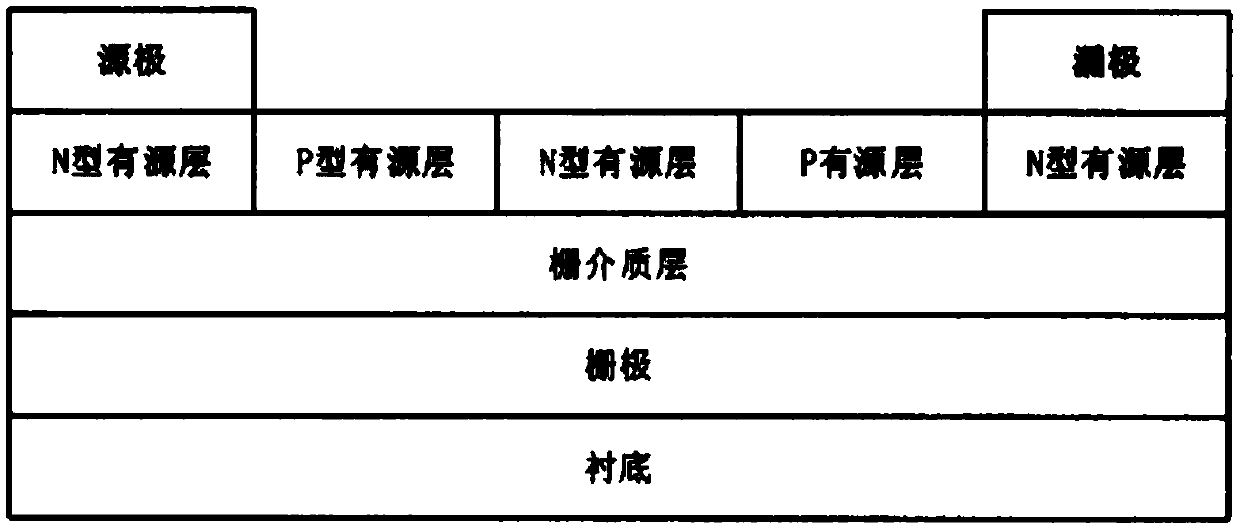
[0010] The present invention uses heavily doped n+-Si / SiO2 as the gate / gate dielectric layer and double as the substrate, C60 as the N-type active layer, pentacene as the P-type active layer, and adopts the bottom-gate bottom-contact structure The preparation process is as follows:

[0011] 1) Clean the n+-Si / SiO2 substrate with a standard process;

[0012] 2) Prepare 3 layers of C60 arranged at intervals on the n+-Si / SiO2 substrate by photolithography as the N-type active layer;

[0013] 3) Prepare two layers of pentacene in the gap between the three layers of N-type active layers by photolithography as the P-type active layer;

[0014] 4) Prepare a metal film (such as gold) on the N-type active layer and P-type active layer arranged side by side by vacuum evaporation as the source and drain electrodes, and the channel length and electrode area are limited by the mask;

[0015] 5) Packaging the manufactured device.

Embodiment 2

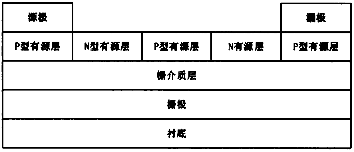
[0017] The present invention uses heavily doped n+-Si / SiO2 as the gate / gate dielectric layer and double as the substrate, C60 as the N-type active layer, pentacene as the P-type active layer, and adopts the bottom-gate bottom-contact structure The preparation process is as follows:

[0018] 1) Clean the n+-Si / SiO2 substrate with a standard process;

[0019] 2) Prepare 3-layer spaced pentacene on n+-Si / SiO2 substrate by photolithography as P-type active layer;

[0020] 3) Prepare 2 layers of C60 as the N-type active layer in the gap between the 3-layer P-type active layer by photolithography;

[0021] 4) Prepare a metal thin film (such as gold) on the P-type active layer and N-type active layer arranged side by side by vacuum evaporation as the source and drain electrodes, and the channel length and electrode area are limited by the mask;

[0022] 5) Packaging the manufactured device.


PUM


Abstract

The invention relates to a bipolar organic field effect transistor. The bipolar organic field effect transistor comprises a substrate, a gate, a gate dielectric layer, an N-type active layer, a P-typeactive layer, a source and a drain, wherein the N-type active layer and the P-type active layer are arranged side by side in a cross mode among the source, the drain and gate dielectric layer to forma vertical laminated structure. The vertical laminated structure can make exciton dissociation at the interface between the N-type active layer and the P-type active layer sufficient so as to improvethe carrier mobility of electrons and holes in the organic bipolar field effect transistor. Therefore, the bipolar organic field effect transistor effectively improves the performances of the bipolarorganic field effect transistor.

Description

technical field [0001] The invention belongs to the technical field of solid electronic devices, in particular to a bipolar organic field effect transistor with a vertical stacked structure. Background technique [0002] A bipolar organic field effect transistor usually consists of a substrate, a gate, a gate dielectric layer, an N-type active layer, a P-type active layer, a source and a drain. Most of the N-type active layer and the P-type active layer are horizontally stacked, that is, the N-type active layer is located between the gate dielectric layer and the P-type active layer or the P-type active layer is located between the gate dielectric layer and the N-type active layer Among them, we call the bipolar organic field effect transistor with this structure a bipolar organic field effect transistor with a horizontal stacking structure. At the same time, most organic semiconductor materials belong to the single-carrier transport type, that is, their mobility for one ty...

Claims


Application Information

Patent Timeline
Patent Type & Authority Applications(China)
IPC IPC(8): H01L51/05
CPCH10K10/486H10K10/466
Inventor 洪越
Owner 仪征市坤翎铝业有限公司
Why Eureka
Try Eureka