Semiconductor device

A semiconductor and conductor technology, applied in the field of impact structure, can solve the problems of defective components and large impact of components, and achieve the effect of suppressing defective components and alleviating impact.

Inactive Publication Date: 2019-04-16
MITSUBISHI ELECTRIC CORP
View PDF1 Cites 2 Cited by
  • Summary
  • Abstract
  • Description
  • Claims
  • Application Information

AI Technical Summary

Problems solved by technology

[0004] However, since Cu wires have a greater impact on the device when bonding to the surface electrodes than Al wires, there is a problem that device defects occur.

Method used


Image

  • Semiconductor device
  • Semiconductor device
  • Semiconductor device

Examples


Embodiment approach 1

[0024]

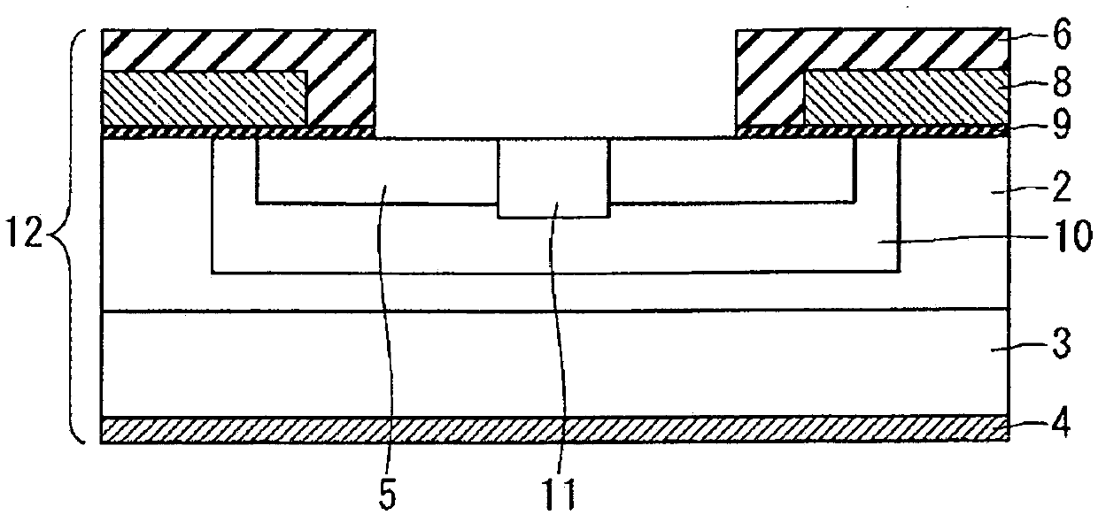
[0025] figure 1 It is a sectional view showing the structure of the power semiconductor element 12 according to Embodiment 1 of the present invention. Hereinafter, the structure of the power semiconductor element 12 will be described. As a substrate of the power semiconductor element 12, a SiC substrate 3 is used, on which an element structure is formed. When a SiC substrate is used, it is possible to fabricate a semiconductor element with low loss and high-speed operation and high-temperature operation, compared with a conventionally used Si substrate. exist figure 1 In , the power semiconductor element 12 is represented as a MOSFET (Metal-Oxide-Semiconductor Field-Effect-Transistor).

[0026] On the front side of SiC substrate 3 , drift layer 2 is formed by epitaxial growth, and on the back side, back electrode 4 electrically connected to SiC substrate 3 is formed. Base region 10 is partially formed on the surface of drift layer 2 , and source region 5 is part...

Embodiment approach 2

[0050]

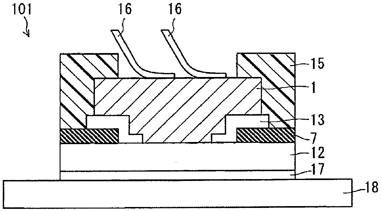
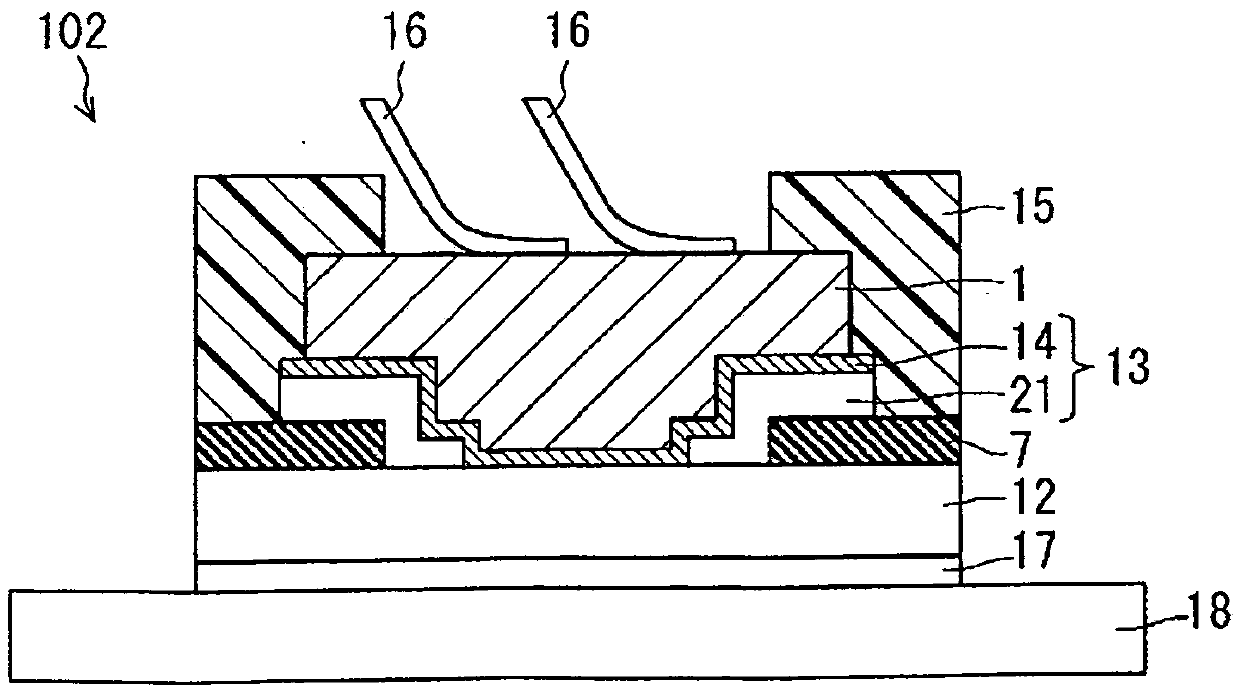
[0051] Figure 4 It is a cross-sectional view showing the structure of the semiconductor device 103 according to Embodiment 2 of the present invention. The semiconductor device 103 uses a fracture toughness value ratio including SiO 2 It is the same as the semiconductor device 102 in that the interlayer insulating film 7 and the large barrier metal layer 14 constitute a part of the stress relieving layer 13, but the barrier metal layer 14 is provided between the interlayer insulating film 7 and the non-barrier metal stress relieving layer 21. One point is different from the semiconductor device 102 . Other than that, the structure of the semiconductor device 103 is the same as that of the semiconductor device 102 .

[0052] In the semiconductor device 102 , the barrier metal layer 14 is provided between the Cu electrode 1 and the non-barrier metal stress relieving layer 21 in order to prevent Cu from the Cu electrode from diffusing in the stress relieving layer 13...

Embodiment approach 3

[0058]

[0059] Figure 5 It is a cross-sectional view showing the structure of the semiconductor device 104 according to Embodiment 3 of the present invention. In Embodiment 1 and Embodiment 2, the stress relaxation layer 13 has an opening on the opening of the interlayer insulating film 7 , and the Cu electrode 1 and the source region 5 of the power semiconductor element 12 are electrically connected through the opening of the stress relaxation layer 13 . connect. In contrast, in Embodiment 3, the stress relaxation layer 13 is formed entirely under the Cu electrode 1 from the opening of the interlayer insulating film 7 to the top of the interlayer insulating film 7 . Even with such a structure, by forming the stress relieving layer 13 with a conductor, the Cu electrode 1 is electrically connected to the source region 5 of the power semiconductor element 12 via the stress relieving layer 13 in the opening of the interlayer insulating film 7 . Examples of the material of t...


PUM


Abstract

The purpose of the present invention is to inhibit cracking in an interlayer insulation film caused by growth of Cu crystal grains. A semiconductor device (101) is provided with: a source region (5);an interlayer insulation film (7) formed on the source region (5) so as to be provided with an opening, the interlayer insulation film (7) comprising silicon oxide; a Cu electrode (1) electrically connected to the source region (5) through the opening in the interlayer insulation film (7), an end part of the Cu electrode (1) being positioned on the interlayer insulation film (7) on the inside of an end part of the interlayer insulation film (7); and a stress relaxation layer (13) formed between the Cu electrode (1) and the interlayer insulation film (7) and provided from the inside to the outside of the end part of the Cu electrode (1), the stress relaxation layer (13) comprising a material having a higher fracture toughness value than the interlayer insulation film (7).

Description

technical field [0001] The present invention relates to a structure for alleviating impact during wire bonding of a semiconductor device. Background technique [0002] SiC (silicon carbide) has a larger band gap than Si (silicon). Therefore, a semiconductor element using SiC can operate at a higher temperature than a semiconductor element using Si that operates at a temperature lower than 200°C. [0003] In semiconductor elements operating at temperatures below 200°C, surface electrodes mainly composed of Al (aluminum) are used, and Al wires are bonded to the surface electrodes. However, when operating these semiconductor elements at temperatures exceeding 200°C, there are surface electrodes and There is a problem that the shape of the lead wire changes and the reliability decreases. Therefore, Cu (copper), which has high reliability at high temperatures, has been studied as a material for surface electrodes and wires instead of Al. [0004] However, since the Cu wire has...

Claims


Application Information

Patent Timeline
Patent Type & Authority Applications(China)
IPC IPC(8): H01L21/3205H01L21/60H01L21/768H01L23/522
CPCH01L21/3205H01L23/522H01L21/768H01L2224/05H01L2224/4847H01L2224/4911H01L2224/02166H01L24/05H01L2224/04042H01L2924/00014H01L29/1608H01L2924/00H01L24/45H01L2924/10272H01L2224/48463H01L2924/13055H01L2224/45147H01L21/32051H01L23/5329H01L2224/05147
Inventor 铃木裕弥冈部博明
Owner MITSUBISHI ELECTRIC CORP
Why Eureka
Try Eureka