Antireflection conductive film with matched refractive index and preparation method thereof

A refractive index matching and anti-reflection technology, which is applied in the field of refractive index matching anti-reflection conductive film and its preparation, can solve problems such as not being used, and achieve high hardness of the film layer, good repeatability of industrial production, film hardness and wear resistance Eclipse effect

Inactive Publication Date: 2019-05-03
昆山福钻新材料科技有限公司
View PDF5 Cites 3 Cited by
  • Summary
  • Abstract
  • Description
  • Claims
  • Application Information

AI Technical Summary

Problems solved by technology

At the same time, diamond is a wide bandgap semiconductor material, and its transmission spectrum can range from ultraviolet to far infrared. It is suitable for the protective film of some optical devices, but it is hardly used in optoelectronic devices.

Method used


Image

  • Antireflection conductive film with matched refractive index and preparation method thereof
  • Antireflection conductive film with matched refractive index and preparation method thereof
  • Antireflection conductive film with matched refractive index and preparation method thereof

Examples


Embodiment 1

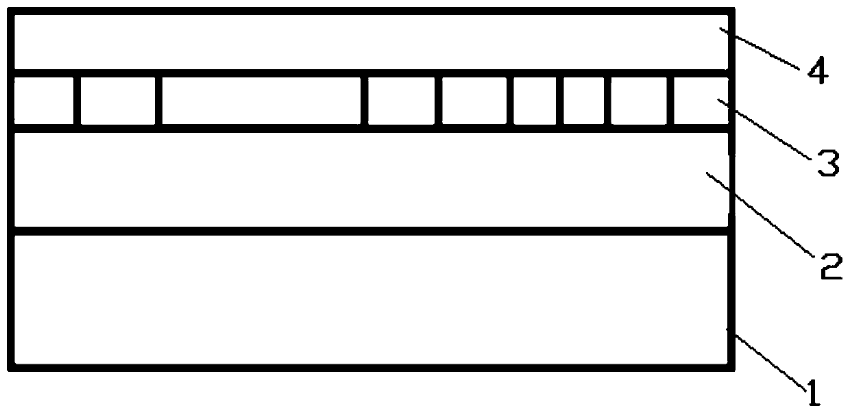
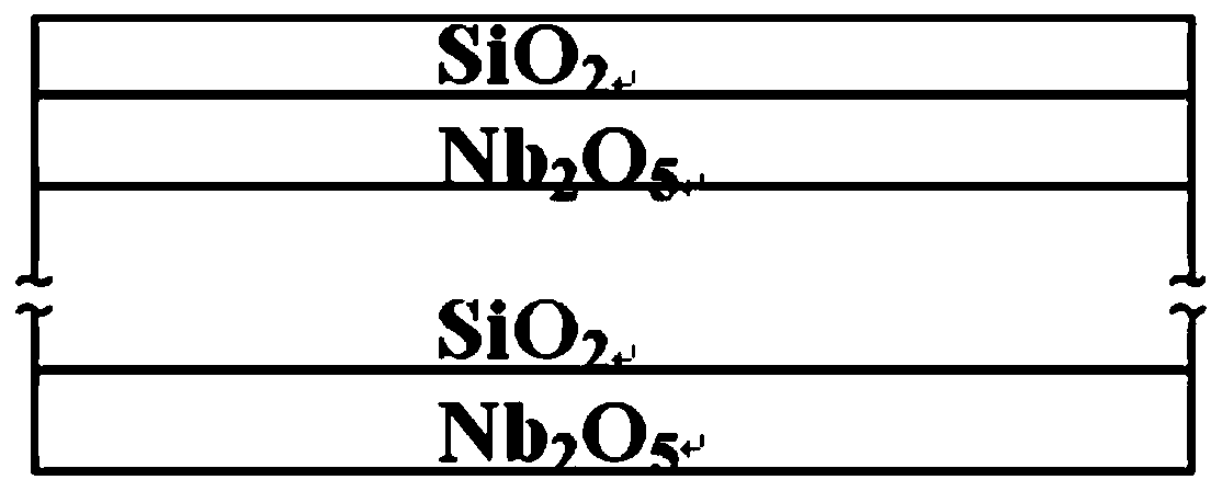
[0046] The anti-reflection layer in the designed film system is a three-layer film, specifically: quartz glass substrate, Nb 2 o 5 Film layer 10nm, SiO 2 Film layer 33nm, Nb 2 o 5 The film layer is 3nm, the ITO film layer is 20nm, and the diamond film layer is 102nm.

[0047] Preparation of Nb 2 o 5 : RF magnetron sputtering or intermediate frequency magnetron sputtering. In RF magnetron sputtering, the sputtering target uses Nb 2 o 5 Target, substrate temperature is room temperature, sample preparation is carried out in a mixed gas with oxygen partial pressure / total pressure of 1~40%, background pressure before sputtering is 2.0×10 -3 Pa, the oxygen-argon ratio is 1 / 10, the sputtering pressure is 0.67Pa, and the sputtering power is 200W. In intermediate frequency magnetron sputtering, the sputtering target is Nb target, the substrate temperature is 150°C, the sample preparation is carried out in a mixed gas with oxygen partial pressure / total pressure of 1~40%, and...

Embodiment 2

[0053] The anti-reflection layer in the designed film system is four-layer film, specifically: quartz glass substrate, Nb 2 o 5 Film layer 6nm, SiO 2 Film layer 50nm, Nb 2 o 5 Film layer 14nm, SiO 2 The film layer is 24nm, the ITO film layer is 20nm, and the diamond film layer is 106nm.

[0054] The preparation method is the same as in Example 1.

Embodiment 3

[0056] The anti-reflection layer in the designed film system is a four-layer film, and the thickness of the diamond layer is increased on the basis of Example 2, specifically: quartz glass substrate, Nb 2 o 5 Film layer 7nm, SiO 2 Film layer 51nm, Nb 2 o 5 Film layer 15nm, SiO 2 The film layer is 23nm, the ITO film layer is 20nm, and the diamond film layer is 130nm.

[0057] The preparation method is the same as in Example 1.


PUM

PropertyMeasurementUnit
thicknessaaaaaaaaaa
thicknessaaaaaaaaaa
refractive indexaaaaaaaaaa

Abstract

The invention discloses an antireflection conductive film with a matched refractive index. The antireflection conductive film is characterized by comprising a glass substrate; an antireflection film layer, an indium tin oxide (ITO) layer and a diamond protective layer are sequentially arranged on the glass substrate, wherein the ITO layer forms an electrode by etching; and the antireflection filmlayer is composed of multiple layers of alternately stacked SiO2 and Nb2O5 oxide dielectric films with different thickness. The invention further discloses a preparation process of the antireflectionconductive film with the matched refractive index. The invention provides the antireflection-indium tin oxide-diamond multilayer film with the matched refractive index and a preparation process thereof, advantages of index matching (IM) and ITO film layers with matched refractive indexes are combined with advantages of the diamond protection layer with good optical characteristics, and the antireflection conductive film can be used for photoelectric devices under various severe environment conditions, so that the usability of the photoelectric devices is improved, and the service life of the photoelectric devices is prolonged.

Description

technical field [0001] The invention belongs to the technical field of refractive index matching anti-reflection-conductive film of photoelectric devices (often referred to as "shadow disappearing glass"), and specifically relates to an anti-reflection film system composed of multiple layers of materials with different refractive indices prepared by magnetron sputtering , Indium tin oxide transparent conductive film was prepared by magnetron sputtering on the anti-reflection film system, diamond film was prepared by plasma CVD on the indium tin oxide film, and the whole anti-reflection-indium tin oxide-diamond multilayer film A preparation method to achieve refractive index matching. Background technique [0002] Tin-doped indium oxide (Indium Tin Oxide, In 2 o 3 : Sn) film, also known as ITO film, has been widely used in flat panel displays, heat mirrors, solar cells and various optoelectronic devices due to its high visible light transmittance, high infrared reflectivity...

Claims


Application Information

Patent Timeline
Patent Type & Authority Applications(China)
IPC IPC(8): C03C17/34
Inventor 沈杰因福明
Owner 昆山福钻新材料科技有限公司
Why Eureka
Try Eureka