Semiconductor structure and forming method thereof

A technology of semiconductor and gate structure, applied in the field of semiconductor structure and its formation, can solve the problems of large parasitic capacitance and large contact resistance, and achieve the effect of reducing contact resistance and increasing contact area

Inactive Publication Date: 2019-05-07
SEMICON MFG INT (SHANGHAI) CORP +1
View PDF13 Cites 3 Cited by
  • Summary
  • Abstract
  • Description
  • Claims
  • Application Information

AI Technical Summary

Problems solved by technology

[0004] However, the semiconductor structure formed in the prior art still has the problem of large conta

Method used


Image

  • Semiconductor structure and forming method thereof
  • Semiconductor structure and forming method thereof
  • Semiconductor structure and forming method thereof

Examples


Embodiment Construction

[0035] There are many problems in the semiconductor structure formed in the prior art, for example, the contact resistance between the metallization and the source-drain doped region is relatively large.

[0036] In combination with a semiconductor structure, the reason why the contact resistance between the metallization and the source-drain doped region is relatively large in the semiconductor structure is analyzed:

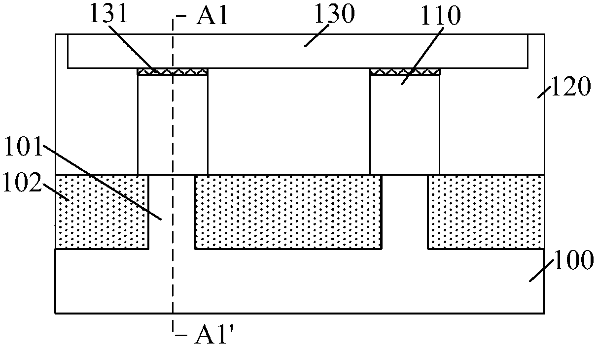
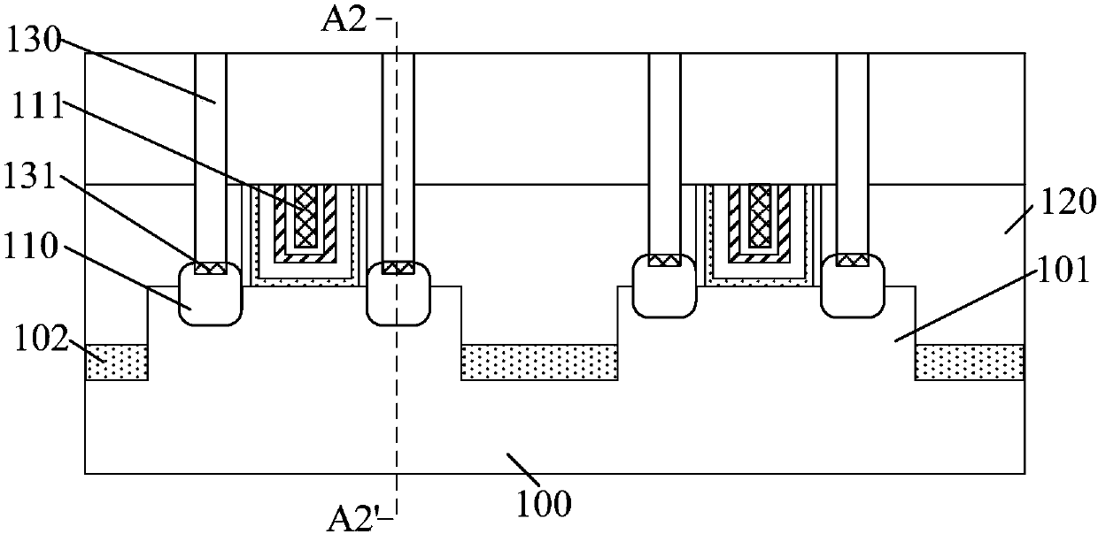
[0037]figure 1 and figure 2 A schematic diagram of a semiconductor structure.

[0038] Please refer to figure 1 and figure 2 , figure 2 yes figure 1 Sectional view along cutting line A1-A1', figure 1 yes figure 2 A cross-sectional view along the cutting line A2-A2', the semiconductor structure includes: a substrate 100 with fins 101 thereon; an isolation structure 102 on the substrate 100, and the isolation structure 102 covers Part of the sidewall of the fin 101, and the surface of the isolation structure 102 is lower than the top surface of the fin...


PUM

PropertyMeasurementUnit
Sizeaaaaaaaaaa
Depthaaaaaaaaaa

Abstract

A semiconductor structure and a forming method thereof are provided. The semiconductor structure comprises a substrate, gate structures, source-drain doping regions, a dielectric layer, a metallide and plugs. The gate structures are located on the substrate, and grooves are respectively arranged in the substrate on the two sides of the gate structures. The source-drain doping regions are located in the bottoms and side walls of the grooves. The dielectric layer is located on the substrate, covers the side walls of the gate structures, and has contact holes. The contact holes are communicated with the grooves. In the direction parallel to the lengthwise direction of the grooves, the size of the grooves is larger than the size of the contact holes. The metallide is located on the bottom andside wall surfaces of the grooves. The plugs are located in the contact holes and the grooves. The metallide is located between the plugs and the source-drain doping regions. The semiconductor structure can reduce the contact resistance between the metallide and the source-drain doping regions.

Description

technical field [0001] The invention relates to the technical field of semiconductor manufacturing, in particular to a semiconductor structure and a forming method thereof. Background technique [0002] With the continuous advancement of semiconductor technology, the feature size of semiconductor devices is gradually reduced. The reduction of critical dimensions means that more transistors can be arranged on the chip, and at the same time, higher requirements are placed on the semiconductor process. [0003] Because metal has good electrical conductivity, in semiconductor technology, the electrical connection between the source and drain doped regions and external circuits is usually realized through metal plugs. However, due to the large difference in the Fermi level between the metal and the semiconductor, the potential barrier between the metal plug and the source-drain doped region is relatively high, resulting in a relatively low contact resistance between the metal pl...

Claims


Application Information

Patent Timeline
IPC IPC(8): H01L29/78H01L29/06H01L21/336
CPCH01L21/76897H01L21/76805H01L21/76814
Inventor 李勇
Owner SEMICON MFG INT (SHANGHAI) CORP
Why Eureka
Try Eureka