Film bulk acoustic wave resonator and a film bulk acoustic wave filter

A thin-film bulk acoustic wave and resonator technology, which is applied in the field of microelectronics, can solve the problems of low power capacity, unsatisfactory compatibility, and large temperature drift, and achieve the effects of high power tolerance, low loss, and small temperature coefficient

Pending Publication Date: 2019-05-14
ZHEJIANG HUAYUAN MICRO ELECTRONICS TECH CO LTD +1
View PDF0 Cites 14 Cited by
  • Summary
  • Abstract
  • Description
  • Claims
  • Application Information

AI Technical Summary

Problems solved by technology

[0004] The purpose of the present invention is to overcome the disadvantages of the prior art, to provide a thin film bulk acoustic resonator and a filter containing the thin film bulk acoustic resonator, to solve the problem of large temperature drift, high loss and power loss in the existing filter. Technical problems such as low capacity and unsatisfactory compatibility

Method used


Image

  • Film bulk acoustic wave resonator and a film bulk acoustic wave filter
  • Film bulk acoustic wave resonator and a film bulk acoustic wave filter
  • Film bulk acoustic wave resonator and a film bulk acoustic wave filter

Examples


preparation example Construction

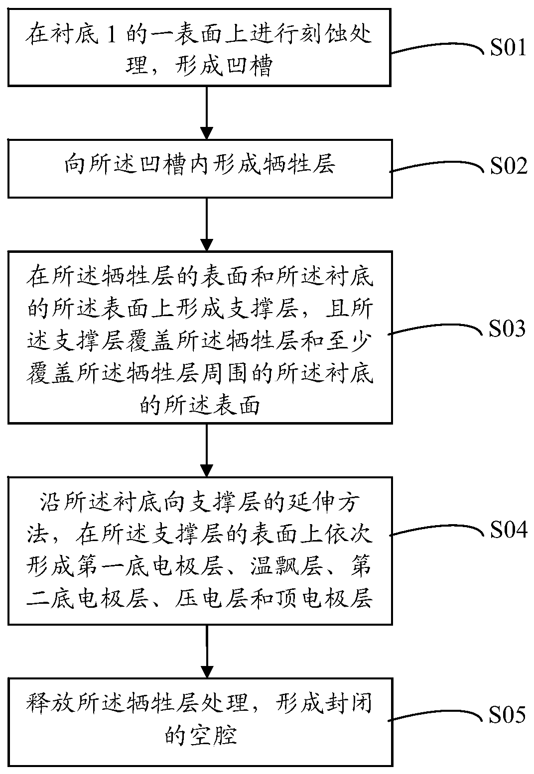
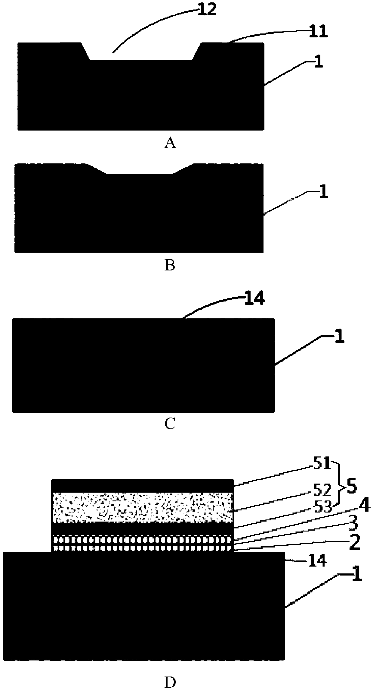
[0034] In addition, the thin-film bulk acoustic resonator described above can be prepared as follows. combine figure 1 with image 3 , the process flow of the preparation method of the thin film bulk acoustic resonator is as follows figure 2 As shown, it includes the following steps:

[0035] S01: Etching is performed on a surface 11 of the substrate 1 to form a groove 12, such as image 3 As shown in A;

[0036] S02: Form a sacrificial layer 14 in the groove 12, such as image 3 Shown in B and 3C;

[0037] S03: Form a supporting layer 2 on the surface of the sacrificial layer 14 and the surface 11 of the substrate 1, and the supporting layer 2 covers the sacrificial layer 14 and at least covers all surrounding areas of the sacrificial layer 14 The surface 11 of the substrate 1; as image 3 as shown in D;

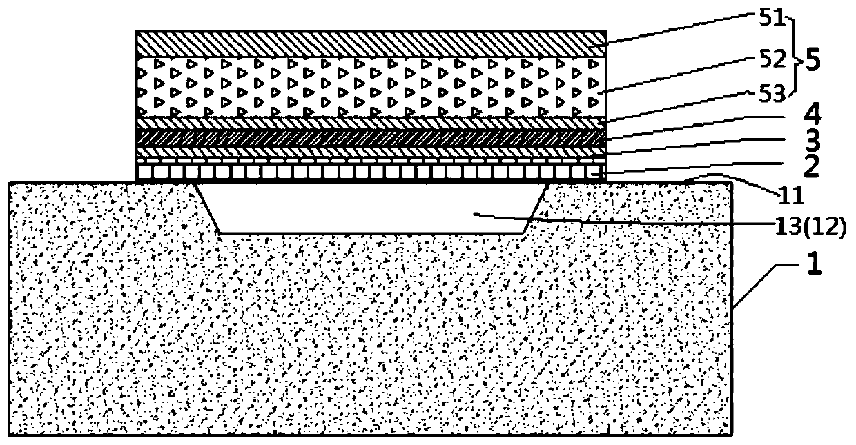
[0038] S04: A method of extending from the substrate 1 to the support layer 2, forming a first bottom electrode layer 3, a temperature floating layer 4, a second b...

Embodiment 11

[0068] This embodiment provides a thin film bulk acoustic resonator. The structure of the thin film bulk acoustic resonator is as figure 1 As shown, the structure of the thin film bulk acoustic resonator is: substrate 1 / support layer 2 / first bottom electrode layer 3 / temperature floating layer 4 / second bottom electrode layer 53 / piezoelectric layer 52 / top electrode layer 51 . Wherein, the substrate 1 is a simple silicon substrate, and the support layer 2 is Si 3 N 4 The film layer has a thickness of 1100 angstroms; the first bottom electrode layer 3 is a Mo film layer with a thickness of 2400 angstroms; the warm floating layer 4 is a fluorine-doped silicon oxide (SiOF) film layer (the content of MgF doping 8%), its thickness is 800 angstroms; the second bottom electrode layer 53 is a Mo film layer, its thickness is 2400 angstroms; the piezoelectric layer 52 is an aluminum nitride film layer of Mg-Hf (Mg and The total Hf doping content is 12%), and its thickness is 11000 angs...

Embodiment 12

[0070] This embodiment provides a thin film bulk acoustic resonator. The structure of the thin film bulk acoustic resonator is as figure 1 As shown, the structure of the thin film bulk acoustic resonator is: substrate 1 / support layer 2 / first bottom electrode layer 3 / temperature floating layer 4 / second bottom electrode layer 53 / piezoelectric layer 52 / top electrode layer 51 . Wherein, the substrate 1 is a simple silicon substrate, and the support layer 2 is Si 3 N 4 The film layer has a thickness of 1200 angstroms; the first bottom electrode layer 3 is a Mo film layer with a thickness of 2500 angstroms; the warm floating layer 4 is a fluorine-doped silicon oxide (SiOF) film layer with a thickness of 800 angstroms The second bottom electrode layer 53 is a Mo film layer with a thickness of 2500 angstroms; the piezoelectric layer 52 is an aluminum nitride film layer of Mg-Hf (doping content is 15%), and its thickness is 11000 angstroms; the top electrode layer 51 is a Mo film l...


PUM


Abstract

The invention discloses a film bulk acoustic wave resonator and a film bulk acoustic wave filter. The thin film bulk acoustic wave resonator comprises a silicon substrate, a support layer and a firstbottom electrode layer, a temperature drift layer and a sandwich piezoelectric stack structure, the supporting layer is combined on the surface, provided with the groove, of the substrate in a laminated manner; a closed cavity is defined by the supporting layer and the groove; wherein the first bottom electrode layer is laminated and combined on the surface, deviating from the substrate, of the supporting layer, the temperature drift layer is laminated and combined on the surface, deviating from the supporting layer, of the first bottom electrode, and the sandwich piezoelectric stack structureis laminated on the surface, deviating from the first bottom electrode layer, of the temperature drift layer. The film bulk acoustic wave filter comprises the film bulk acoustic wave resonator. The film bulk acoustic wave filter and the resonator are low in consumption, small in temperature coefficient, low in temperature drift, high in power bearing capacity, high in working frequency, high in electromechanical coupling coefficient, good in compatibility and good in Q value.

Description

technical field [0001] The invention belongs to the technical field of microelectronics, and in particular relates to a film bulk acoustic wave resonator and a filter. Background technique [0002] Today, with the rapid development of radio communication technology, traditional single-band single-standard equipment is far from being able to meet the diverse requirements of communication systems. New smartphones and personal portable computers no longer only provide basic voice communication functions, but also are compatible with a large number of data interfaces such as digital cameras, MP3, GPS, Bluetooth, and WiFi, and are changing to multi-functional communication terminals. At the same time, with the development of 5G technology, the communication system is becoming more and more multi-band, showing the coexistence of WCDMA, GSM, CDMA and other forms, which requires the communication terminal to be able to accept each frequency band to meet different communication servi...

Claims


Application Information

Patent Timeline
Patent Type & Authority Applications(China)
IPC IPC(8): H03H3/02H03H3/04H03H9/02H03H9/17
Inventor 刘绍侃李善斌史晓婷霍俊标张雪奎董谦
Owner ZHEJIANG HUAYUAN MICRO ELECTRONICS TECH CO LTD
Why Eureka
Try Eureka