Improving method of thickness uniformity of silicon-based epitaxial wafer

A technology of uniform thickness and epitaxial wafers, applied in chemical instruments and methods, from chemical reactive gases, gaseous chemical plating, etc., can solve problems such as uneven thickness distribution of epitaxial wafers, achieve uniformity of film thickness, improve warping The effect of reducing curvature and film thickness variation

Active Publication Date: 2019-05-24
LATTICE POWER (JIANGXI) CORP
View PDF10 Cites 2 Cited by
  • Summary
  • Abstract
  • Description
  • Claims
  • Application Information

AI Technical Summary

Problems solved by technology

[0003] In order to overcome the above shortcomings, the present invention provides a method for improving the thickness uniformity of silicon-based epitaxial wafers, which effectively solves the uneven thickness distribution of epitaxial wafers caused by the use of MOCVD high-speed system in the prior art to grow epitaxial wafers on the surface of silicon substrates technical issues

Method used


Image

  • Improving method of thickness uniformity of silicon-based epitaxial wafer
  • Improving method of thickness uniformity of silicon-based epitaxial wafer
  • Improving method of thickness uniformity of silicon-based epitaxial wafer

Examples


Embodiment 1

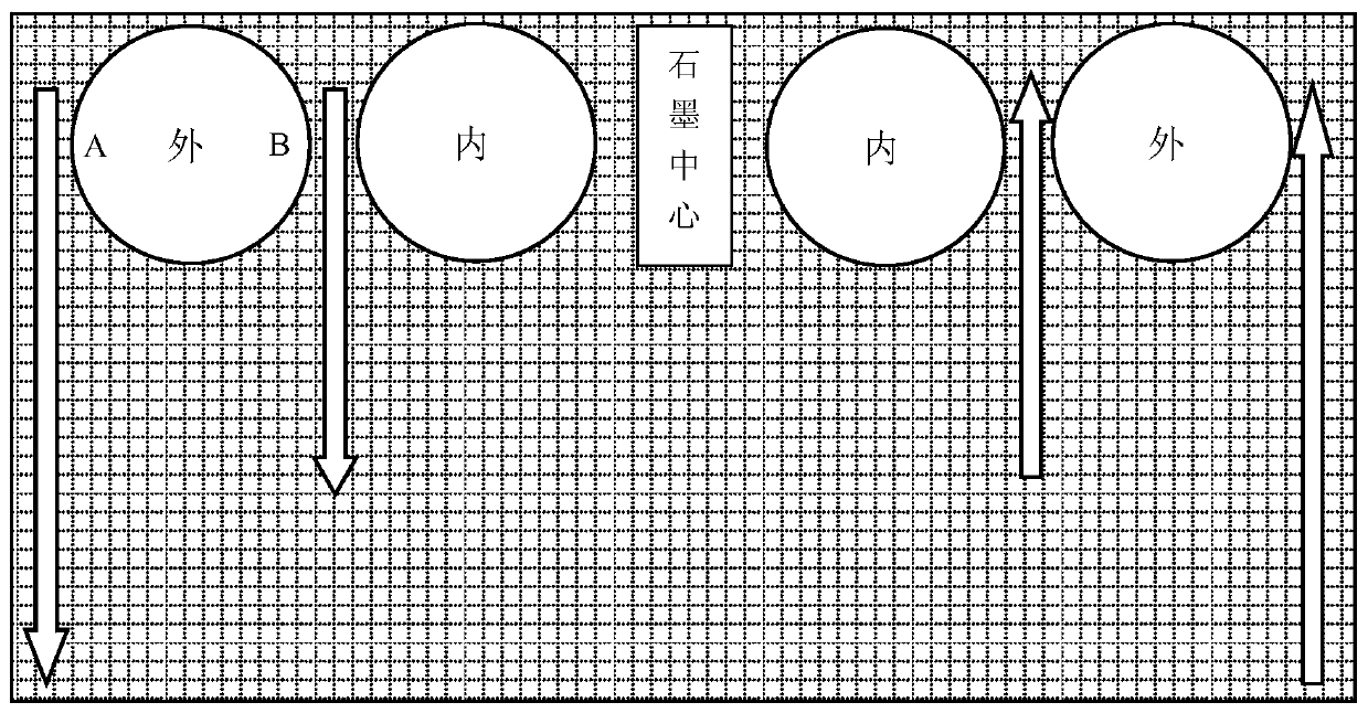
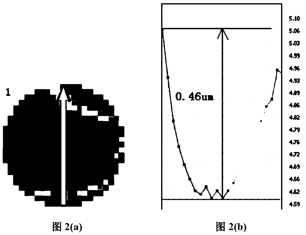
[0020] 1. Place the silicon substrate with (111) crystal orientation on a graphite disk and send it into the reaction chamber, and heat it to 1000°C to grow a 1.5μm thick AlN / AlGaN buffer layer;

[0021] 2. Raise the temperature to 1050° C., and grow a 1 μm thick undoped GaN layer (uGaN).

[0022] 3. A 2 μm thick n-type Si-doped GaN layer is grown on the non-doped GaN layer, that is, an n-type GaN layer. The growth conditions are: pressure 150Torr, temperature 1050°C, graphite disk speed 1200r / min, N 2 、H 2 and NH 3 The flow rates are 64L / min, 120L / min and 50L / min respectively.

[0023] figure 2 Shown is the outer ring of the graphite disc ( figure 1 A schematic diagram of the thickness of the n-type GaN layer grown on a wafer placed in the outer ring of the graphite disk), wherein, figure 2 (a) is a schematic diagram of the surface thickness of the wafer, figure 2 (b) is the thickness diagram of each point in the direction of the arrow. It can be seen from the figur...

Embodiment 2

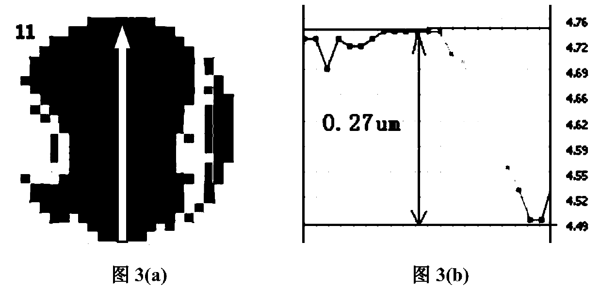
[0026] 1. Place the silicon substrate with (111) crystal orientation on a graphite disk and send it into the reaction chamber, and heat it to 1000°C to grow a 1.5um thick AlN / AlGaN buffer layer;

[0027] 2. Raise the temperature to 1050°C and grow a 1μm undoped GaN layer (uGaN);

[0028] 3. A 2 μm n-type Si-doped GaN layer is grown on the non-doped GaN layer, that is, an n-type GaN layer. The growth conditions are: pressure 150Torr, temperature 1050°C, graphite rotation speed 500r / min, N 2 、H 2 and NH 3 The flow rates are 10L / min, 70L / min and 45L / min respectively.

[0029] Figure 4 Shown is the outer ring of the graphite disc ( figure 1 A schematic diagram of the thickness of the n-type GaN layer grown on a wafer placed in the outer ring of the graphite disk), wherein, Figure 4 (a) is a schematic diagram of the surface thickness of the wafer, Figure 4 (b) is the thickness map of each point in the direction of the arrow. It can be seen from the figure that along the d...


PUM


Abstract

The invention provides an improving method of the thickness uniformity of a silicon-based epitaxial wafer. The improving method is characterized by being suitable for an MOCVD high-rotating-speed system and comprising the steps: in the process of epitaxial growth of a GaN layer on the surface of a silicon substrate, the rotating speed of a graphite disc is adjusted to be 500-1200 r / min, a matchedair flow is introduced according to the rotating speed of the graphite disc, and the corresponding temperature and pressure are controlled. According to the improving method, the thickness uniformityof the wafer can be improved, the technical problem of the film thickness uniformity of the silicon-based epitaxial wafer is effectively solved, and in practical application, the film thickness deviation improved through the improving method can be decreased by 40% or above.

Description

technical field [0001] The invention relates to the technical field of semiconductors, in particular to a method for improving the thickness uniformity of silicon-based epitaxial wafers. Background technique [0002] MOCVD (metal organic compound chemical vapor deposition) machines are divided into high-speed and low-speed systems. The machines of the low-speed system include the Crius series and the G series of the German AIXTRON company, which have the advantage of good uniformity; the high-speed systems include the United States The K series of VEECO company and the D480 and A7 machines of China Micro-Semiconductor Co., Ltd., due to the large difference in the linear speed of the wafer at different positions in the system, cause large airflow differences, which in turn lead to uneven distribution of the surface thickness of the same wafer, such as figure 1 As shown, the thickness difference between A and B on the surface of the same wafer is relatively large. Furthermore...

Claims


Application Information

Patent Timeline
Patent Type & Authority Applications(China)
IPC IPC(8): C23C16/30C23C16/458C30B25/12C30B29/40
Inventor 涂逵
Owner LATTICE POWER (JIANGXI) CORP
Why Eureka
Try Eureka