Semiconductor structures and methods of forming them

A semiconductor and gate structure technology, applied in the field of semiconductor structure and its formation, can solve problems such as poor performance of fin field effect transistors, and achieve the effects of good performance, reduced contact resistance, and suppression of short channel effects

Active Publication Date: 2022-03-22
SEMICON MFG INT (SHANGHAI) CORP +1
View PDF3 Cites 0 Cited by
  • Summary
  • Abstract
  • Description
  • Claims
  • Application Information

AI Technical Summary

Problems solved by technology

[0004] However, the performance of fin field effect transistors prepared by the prior art is still poor

Method used


Image

  • Semiconductor structures and methods of forming them
  • Semiconductor structures and methods of forming them
  • Semiconductor structures and methods of forming them

Examples


Embodiment Construction

[0033] As mentioned in the background, FinFETs have poor performance.

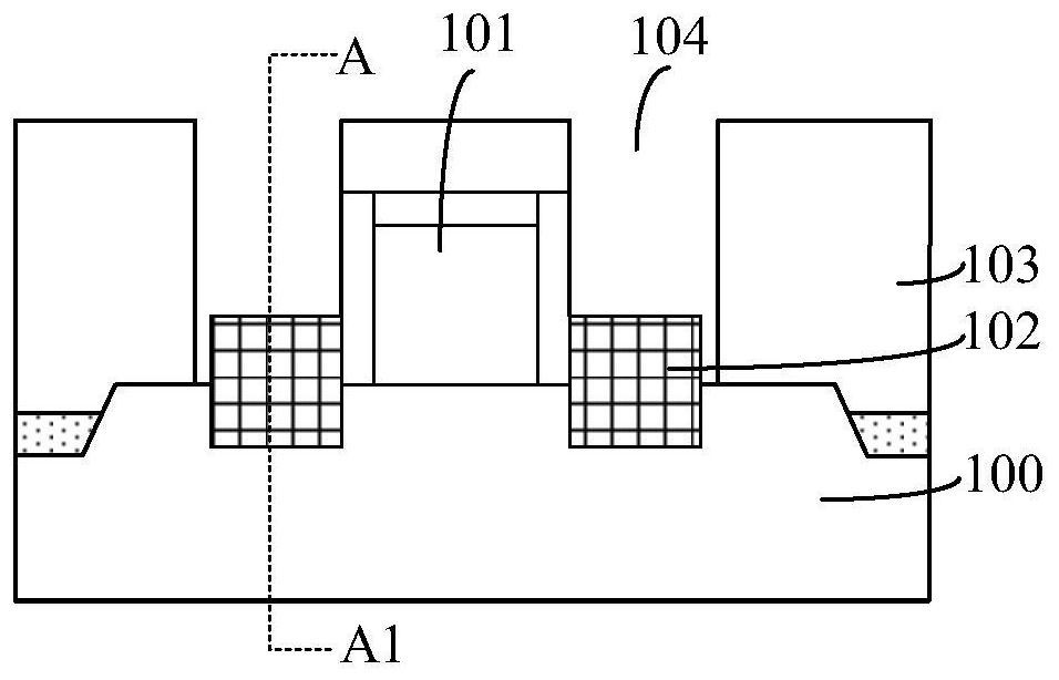
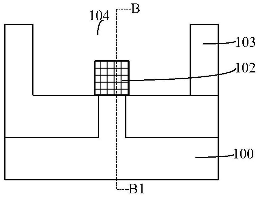
[0034] figure 1 with figure 2 It is a schematic diagram of the structure of a fin field effect transistor.

[0035] Please refer to figure 1 with figure 2 , figure 2 yes figure 1 A schematic sectional view along line A-A1, figure 1 yes figure 2 A schematic cross-sectional view along the line B-B1, a substrate 100 with a gate structure 101 on it; source and drain doped regions 102 located in the substrate 100 on both sides of the gate structure 101; located on the substrate 100 and the gate structure 101 The above dielectric layer 103 has a contact hole 104 exposing the source-drain doped region 102 in the dielectric layer 103 .

[0036] In the above structure, with the continuous improvement of the integration degree of semiconductor devices, the size of the source-drain doped region 102 is continuously reduced, so that the subsequent contact area between the plug in the contact hole 104 and th...


PUM

PropertyMeasurementUnit
thicknessaaaaaaaaaa

Abstract

A semiconductor structure and a method for forming the same, wherein the method includes: providing a substrate, and the substrate includes a first region; forming a first gate structure and a first gate structure located in the substrate on both sides of the first gate structure on the substrate of the first region; A source-drain doped region, the first source-drain doped region has first dopant ions, and the first doped ion in the first source-drain doped region has a first atomic percentage concentration; forming a first gate After the electrode structure and the first source-drain doped region, a first improved layer is formed on the top of the first source-drain doped region, and the first doped ion in the first improved layer has a second atomic percentage concentration, and the The second atomic percent concentration is greater than the first atomic percent concentration. The semiconductor device formed by the method can not only reduce the contact resistance between the first source-drain doped region and the subsequently formed plug, but also suppress the short channel effect.

Description

technical field [0001] The invention relates to the field of semiconductor manufacturing, in particular to a semiconductor structure and a forming method thereof. Background technique [0002] With the continuous development of semiconductor technology, the improvement of integrated circuit performance is mainly achieved by continuously shrinking the size of integrated circuit devices to increase its speed. Currently, the fabrication of semiconductor devices is constrained by various physical limits due to the pursuit of high device density, high performance, and low cost in semiconductor processes and progress to nanotechnology process nodes. [0003] Manufacturing and design challenges as CMOS devices continue to shrink have prompted the development of three-dimensional designs such as Fin Field Effect Transistors (FinFETs). Compared with the existing planar transistors, the fin field effect transistor has more superior performance in terms of channel control and reducing...

Claims


Application Information

Patent Timeline
Patent Type & Authority Patents(China)
IPC IPC(8): H01L21/336H01L29/78H01L29/06
Inventor 李勇
Owner SEMICON MFG INT (SHANGHAI) CORP
Why Eureka
Try Eureka