Unlock instant, AI-driven research and patent intelligence for your innovation.

Array substrate and manufacturing method thereof, display panel, electronic device

The technology of an array substrate and a flexible substrate is applied in the field of electronic equipment, array substrate and its manufacturing method, and display panel, and can solve the problems of capacitor leakage, uneven gray scale of the display panel, and high leakage current, and achieve the improvement of gray scale uniformity, Weaken the effect of floating body and reduce the effect of leakage current

Active Publication Date: 2021-03-16
BOE TECH GRP CO LTD
View PDF9 Cites 0 Cited by
  • Summary
  • Abstract
  • Description
  • Claims
  • Application Information

AI Technical Summary

Problems solved by technology

[0004] In view of this, an embodiment of the present invention provides an array substrate and its manufacturing method, a display panel, and a method for electronic equipment. The floating body effect causes capacitor leakage, which in turn affects the circuit compensation circuit, and finally leads to the problem of uneven gray scale of the display panel

Method used


Image

  • Array substrate and manufacturing method thereof, display panel, electronic device
  • Array substrate and manufacturing method thereof, display panel, electronic device
  • Array substrate and manufacturing method thereof, display panel, electronic device

Examples


Embodiment 1

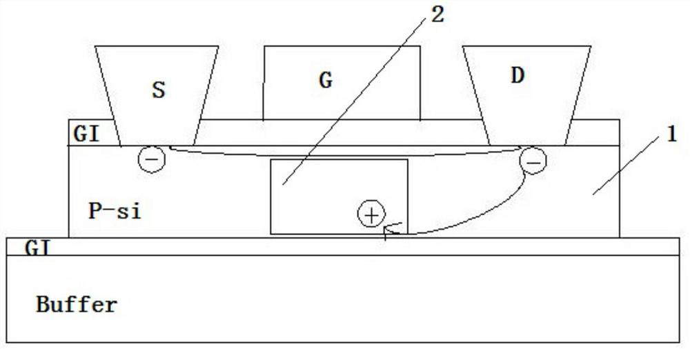
[0042] Reference attached figure 2 , an array substrate provided by an embodiment of the present invention, which includes a driving TFT and a switching TFT,

[0043] Wherein, the driving TFT includes a polysilicon layer 3, a top gate 4 and a bottom gate 5;

[0044] Both ends of the polysilicon layer 3 are electrically connected to the source S and the drain D respectively;

[0045] The top gate 4 and the bottom gate 5 are respectively arranged on the upper side and the lower side of the polysilicon layer 3 for reducing the floating body effect between the drain D and the source S.

[0046] Specifically, in order to solve the problem that the leakage current of the polysilicon active layer material in the LTPO process is too high, and the floating body effect is prone to occur during the application process to cause capacitance leakage, which in turn affects the circuit compensation circuit, and finally leads to uneven gray levels of the display panel. Problem, the present i...

Embodiment 2

[0061] Further, refer to the attached Figure 5 , a method for manufacturing an array substrate provided by an embodiment of the present invention, in a specific implementation, includes the following steps:

[0062] It should be noted that this embodiment is aimed at the case where the top gate 4 is set as indium gallium zinc oxide (IGZO), and the bottom gate 5 is set as a metal gate (Gate-1):

[0063] S1. Coating a flexible substrate 13 on a glass substrate to form a flexible substrate 9, and making a bottom gate 4 on the upper side of the flexible substrate 9;

[0064] S2, depositing silicon on the upper side of the bottom gate 4 and performing polycrystallization and patterning treatment to form a polysilicon layer 3;

[0065] S3, sputtering the top gate 5 on the upper side of the polysilicon layer 3 and patterning it;

[0066] S4 , making through holes 14 for source S and drain D (Drain) on the upper side of the top gate 5 , sputtering and patterning the through holes 1...

Embodiment 3

[0078] Further, refer to the attached Image 6 , a method for manufacturing an array substrate provided by an embodiment of the present invention, in a specific implementation, includes the following steps:

[0079] It should be noted that in this embodiment, the top gate 4 is set as a metal gate (Gate-1) and kept on the upper side of the polysilicon layer 3, and the bottom gate is added on the lower side of the polysilicon layer 3. The case of pole 5 (Gate-3):

[0080] Coating polyimide (PI) on a glass substrate (Glass) as a flexible substrate 9, depositing silicon oxide on the flexible substrate 9 as a first buffer layer (Buffer-o) 8, then sputtering a metal layer and doing Patterning to form the bottom gate 5 (Gate-3), and then depositing the first insulating layer GI1 (Gate insulator) 6;

[0081] After depositing amorphous Si on the first insulating layer GI1 (Gate insulator) 6, perform laser annealing (ELA) treatment to form polysilicon (Poly-Si), and then perform patte...


PUM


Abstract

The invention discloses an array substrate and a manufacturing method thereof, a display panel and electronic equipment, and relates to the technical field of electronic display equipment. It solves the problem that the leakage current of the polycrystalline silicon active layer material in the LTPO process is too high and the floating body effect is prone to occur during the application process. This causes capacitor leakage, which in turn affects the circuit compensation circuit, ultimately leading to the problem of uneven gray scale on the display panel. The main technical solution of the present invention is: an array substrate, which includes a driving TFT and a switching TFT: wherein the driving TFT includes a polysilicon layer, a top gate and a bottom gate; both ends of the polysilicon layer are electrically connected to the source and drain electrodes respectively. Connection; the top gate and bottom gate are respectively arranged on the upper and lower sides of the polysilicon layer to reduce the floating body effect between the drain and the source. The present invention changes the top gate structure of the traditional driving TFT to a double gate structure including a top gate and a bottom gate, shields the influence of the drain electric field on the channel and source, reduces the leakage current, weakens the floating body effect, and promotes The gray scale uniformity of the display panel is improved.

Description

technical field [0001] The present invention relates to the technical field of electronic display equipment, in particular to an array substrate and a manufacturing method thereof, a display panel, and electronic equipment. Background technique [0002] In the field of display technology, a thin film transistor (Thin Film Transistor, TFT) means that each liquid crystal pixel on a liquid crystal display is driven by a TFT integrated behind it, so as to achieve high-speed, high-brightness and high-contrast display screen information; especially Large-size, high-resolution and high-quality flat-panel display devices, such as LCD TVs, have occupied a dominant position in the current flat-panel display market; with OLED (Organic Light-Emitting Diode) organic light-emitting diodes in display screens With the development of application technology, people have higher and higher requirements for low power consumption performance of display devices. The LTPS (Low Temperature Polysilic...

Claims


Application Information

Patent Timeline
Patent Type & Authority Patents(China)
IPC IPC(8): H01L27/12H01L29/786H01L21/77
CPCH01L27/1225H01L27/1251H01L29/78648
Inventor 秦斌彭锦涛彭宽军张方振牛亚男
Owner BOE TECH GRP CO LTD