Check patentability & draft patents in minutes with Patsnap Eureka AI!

GaN-based light-emitting diode epitaxial wafer and manufacturing method thereof

A light-emitting diode, gallium nitride-based technology, applied in semiconductor/solid-state device components, semiconductor devices, electrical components, etc., can solve problems affecting electronic expansion, improve antistatic ability, improve warpage, and promote horizontal expansion Effect

Active Publication Date: 2021-10-08
HC SEMITEK ZHEJIANG CO LTD
View PDF3 Cites 0 Cited by
  • Summary
  • Abstract
  • Description
  • Claims
  • Application Information

AI Technical Summary

Problems solved by technology

[0008] The embodiment of the present invention provides a gallium nitride-based light-emitting diode epitaxial wafer and its manufacturing method, which can solve the problem that many defects in the N-type semiconductor layer in the prior art will affect the expansion of electrons

Method used


Image

  • GaN-based light-emitting diode epitaxial wafer and manufacturing method thereof
  • GaN-based light-emitting diode epitaxial wafer and manufacturing method thereof
  • GaN-based light-emitting diode epitaxial wafer and manufacturing method thereof

Examples


Embodiment Construction

[0028] In order to make the object, technical solution and advantages of the present invention clearer, the implementation manner of the present invention will be further described in detail below in conjunction with the accompanying drawings.

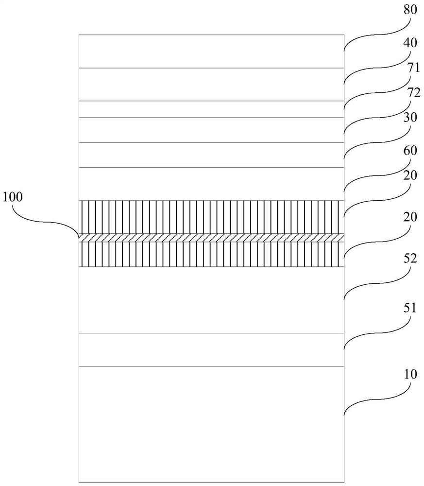
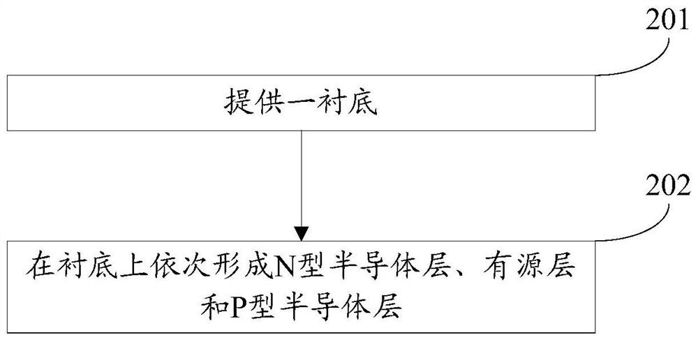
[0029] An embodiment of the present invention provides a GaN-based light-emitting diode epitaxial wafer. figure 1 A schematic structural diagram of a gallium nitride-based light-emitting diode epitaxial wafer provided by an embodiment of the present invention. see figure 1 , the GaN-based light-emitting diode epitaxial wafer includes a substrate 10, an N-type semiconductor layer 20, an active layer 30, and a P-type semiconductor layer 40, and the N-type semiconductor layer 20, the active layer 30, and the P-type semiconductor layer 40 are sequentially stacked on the substrate 10.

[0030] In this embodiment, the N-type semiconductor layer 20 is a GaN layer doped with Si. Such as figure 1 As shown, at least one composite layer 100 i...


PUM

PropertyMeasurementUnit
thicknessaaaaaaaaaa
thicknessaaaaaaaaaa
thicknessaaaaaaaaaa

Abstract

The invention discloses a gallium nitride-based light-emitting diode epitaxial wafer and a manufacturing method thereof, belonging to the technical field of semiconductors. The gallium nitride-based light-emitting diode epitaxial wafer includes a substrate, an N-type semiconductor layer, an active layer, and a P-type semiconductor layer, and the N-type semiconductor layer, the active layer, and the P-type semiconductor layer are sequentially stacked on On the substrate; the N-type semiconductor layer is a Si-doped GaN layer; at least one composite layer is inserted in the N-type semiconductor layer, and the composite layer includes a first sub-layer, a second sub-layer stacked in sequence layer and a third sublayer; the first sublayer is a Mg-doped GaN layer, the second sublayer is an undoped AlGaN layer, and the third sublayer is a Ge-doped GaN layer. The invention can effectively promote the lateral expansion of electrons, make the electrons evenly distributed in the N-type semiconductor layer, and improve the antistatic ability of the LED.

Description

technical field [0001] The invention relates to the technical field of semiconductors, in particular to a gallium nitride-based light-emitting diode epitaxial wafer and a manufacturing method thereof. Background technique [0002] A light-emitting diode (English: Light Emitting Diode, referred to as: LED) is a semiconductor electronic component that can emit light. LED has attracted widespread attention due to its advantages of energy saving, environmental protection, high reliability, and long service life. Since civil lighting focuses on energy saving and service life of products, it is particularly critical to reduce the series resistance of LEDs and improve the antistatic ability of LEDs. [0003] Epitaxial wafers are the primary products in the LED manufacturing process. The existing LED epitaxial wafer includes a substrate, an N-type semiconductor layer, an active layer and a P-type semiconductor layer, and the N-type semiconductor layer, the active layer and the P-t...

Claims


Application Information

Patent Timeline
Patent Type & Authority Patents(China)
IPC IPC(8): H01L33/14H01L33/02H01L33/00H01L23/60
Inventor 葛永晖郭炳磊王群吕蒙普李鹏
Owner HC SEMITEK ZHEJIANG CO LTD
Features
  • R&D
  • Intellectual Property
  • Life Sciences
  • Materials
  • Tech Scout
  • Unparalleled Data Quality
  • Higher Quality Content
  • 60% Fewer Hallucinations
Learn More