Capacitive-coupled non-volatile thin-film transistor strings in three dimensional arrays

A technology for storing transistors and thin films, which is applied in the direction of electric solid-state devices, circuits, electrical components, etc.

Pending Publication Date: 2019-06-07
SUNRISE MEMORY CORP
View PDF21 Cites 6 Cited by
  • Summary
  • Abstract
  • Description
  • Claims
  • Application Information

AI Technical Summary

Problems solved by technology

In this case, conventional non-volatile memory has a data retention time in excess of decades

Method used


Image

  • Capacitive-coupled non-volatile thin-film transistor strings in three dimensional arrays
  • Capacitive-coupled non-volatile thin-film transistor strings in three dimensional arrays
  • Capacitive-coupled non-volatile thin-film transistor strings in three dimensional arrays

Examples


Embodiment Construction

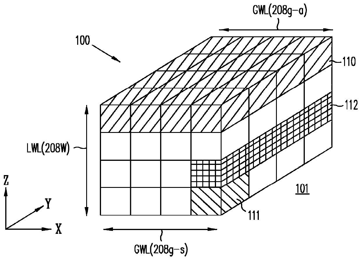
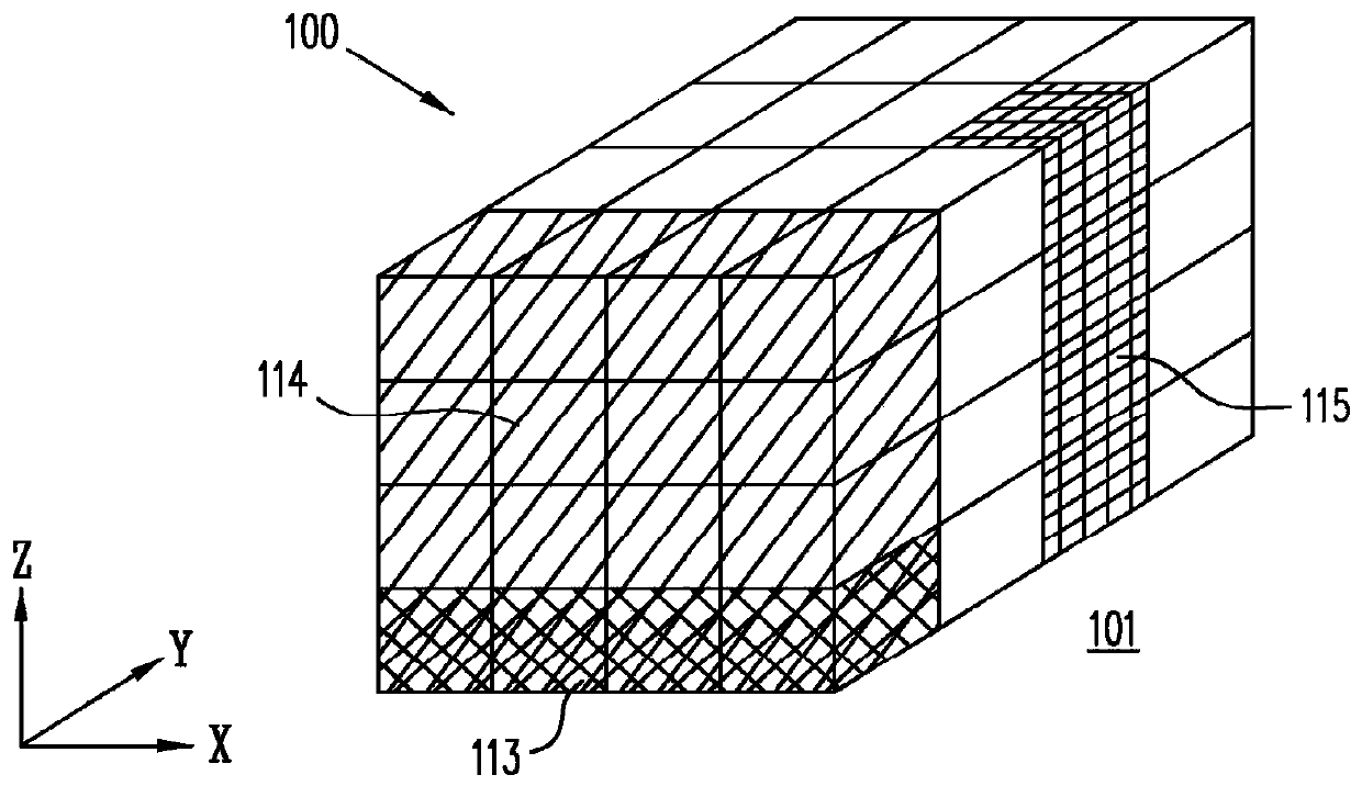
[0068] Figure 1a-1 and 1a-2 A conceptual memory structure 100 is shown, and the organization of memory cells according to embodiments of the invention is illustrated in this detailed description. Such as Figure 1a-1 As shown, memory structure 100 represents a three-dimensional memory array or block of memory cells formed in a deposited film fabricated on the surface of substrate layer 101 . Substrate layer 101 may be familiar to those of ordinary skill in the art, for example, a conventional silicon wafer used in the manufacture of integrated circuits. In this detailed description, a Cartesian coordinate system such as Figure 1a-1 ) are for illustrative purposes only. In this coordinate system, the surface of the substrate layer 101 is regarded as a plane parallel to the XY plane. Thus, as used in this specification, the term "horizontal" refers to any direction parallel to the XY plane, while the term "vertical" refers to the Z direction. As shown, block 100 is composed...


PUM


Abstract

Multi-gate NOR flash thin-film transistor (TFT) string arrays are organized as three dimensional stacks of active strips. Each active strip includes a shared source sublayer and a shared drain sublayer that is connected to substrate circuits. Data storage in the active strip is provided by charge-storage elements between the active strip and a multiplicity of control gates provided by adjacent local word-lines. The parasitic capacitance of each active strip is used to eliminate hard-wire ground connection to the shared source making it a semi-floating, or virtual source. Pre-charge voltages temporarily supplied from the substrate through a single port per active strip provide the appropriate voltages on the source and drain required during read, program, program-inhibit and erase operations. TFTs on multiple active strips can be pre-charged separately and then read, programmed or erased together in a massively parallel operation.

Description

[0001] Cross References to Related Applications [0002] This application is related to, and claims priority to, the following patents, (i) Serial No. 62 / 235,322 filed September 30, 2015, entitled "Multi-Gate Arranged in Stacked Horizontal Active Strips with Vertical Control Gates Multi-gate NOR Flash Thin-film Transistor Strings Arranged in Stacked Horizontal Active Strips With Vertical Control Gates" ("Co-Pending Provisional Application I"); (ii ) U.S. Provisional Patent Application Serial No. 62 / 260,137, entitled "Three-dimensional Vertical NOR Flash Thin-film Transistor Strings," filed November 25, 2015 ("Co-Pending Provisional Application II"); (iii) Serial No. 15 / 220,375, filed July 26, 2016, entitled "Multi-Gate NOR Flash Thin Film Transistors Arranged in Stacked Horizontal Active Stripes with Vertical Control Gates Strings (Multi-Gate NOR Flash Thin-film Transistor Strings Arranged in Stacked Horizontal Active Strips With Vertical Control Gates)", the U.S. non-provision...

Claims


Application Information

Patent Timeline
Patent Type & Authority Applications(China)
IPC IPC(8): H01L21/02H01L21/28H01L21/768H01L21/3213H01L23/528H01L29/06H01L29/08H01L29/10H01L29/423H01L29/51H01L29/66
CPCH10B43/30H10B43/20G11C16/08G11C16/10H01L21/28H01L29/78618H01L29/78696H01L2924/1443H10B41/30H10B41/20
Inventor E.哈拉里
Owner SUNRISE MEMORY CORP
Why Eureka
Try Eureka