

Sputtering method
A thin film and nitride technology, applied in the field of sputtering, can solve the problems of increased cost and the inability to obtain the protective properties of silicon nitride, and achieve the effects of film formation speed, low cost and high reliability
- Summary
- Abstract
- Description
- Claims
- Application Information
AI Technical Summary
Problems solved by technology
Method used
Image

Examples
Embodiment approach 1
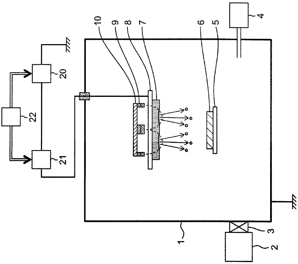
[0046] First, the main reference figure 1 The structure of the sputtering apparatus according to the first embodiment of the present disclosure will be described.
[0047] figure 1 It is a cross-sectional view showing a schematic configuration of the sputtering device of the first embodiment. The sputtering apparatus of Embodiment 1 includes a vacuum chamber 1, a vacuum pump 2, a gas supply source 4, a back plate 8, a DC power supply 20, a pulsing unit 21, a power supply / pulse controller 22 functioning as an example of a control unit, and a substrate Holder 5.
[0048] The vacuum chamber 1 has a structure in which the inside of the vacuum chamber 1 is decompressed to a vacuum state by exhausting with a vacuum pump 2 connected via a gate valve 3.
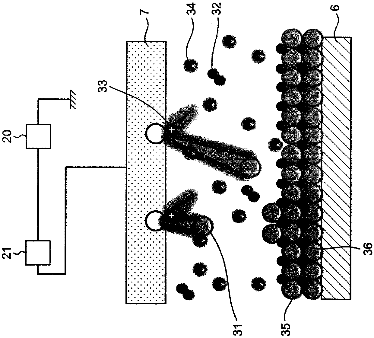
[0049] The gas supply source 4 can supply the gas required for sputtering to the vacuum chamber 1 at a constant speed. As the gas supplied from the gas supply source 4, for example, a gas reactive with a target material such as nitrogen...
PUM
| Property | Measurement | Unit |
|---|---|---|
| refractive index | aaaaa | aaaaa |
Abstract
Description
Claims
Application Information