Broadband metamaterial wave-absorbing device

A metamaterial and absorber technology, applied in electrical components, antennas, etc., can solve the problems of narrow absorption frequency band and limited practical application, and achieve the effect of small structural restrictions, easy implementation, and flexible design methods.

Inactive Publication Date: 2019-06-11
CHINA ELECTRONIC TECH GRP CORP NO 38 RES INST
View PDF2 Cites 8 Cited by
  • Summary
  • Abstract
  • Description
  • Claims
  • Application Information

AI Technical Summary

Problems solved by technology

Most of the existing metamaterial absorbers deal with a single frequency or multiple frequencies, and the absorbing frequency band is narrow, so the practical application is limited

Method used


Image

  • Broadband metamaterial wave-absorbing device
  • Broadband metamaterial wave-absorbing device
  • Broadband metamaterial wave-absorbing device

Examples


Embodiment 1

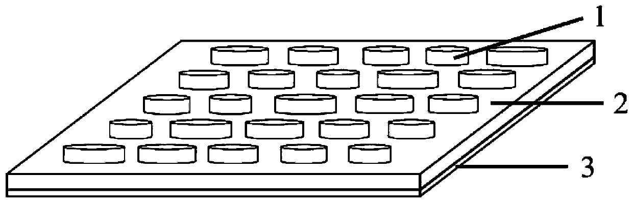
[0025] like figure 1 , 2 As shown in , 3, the broadband metamaterial wave absorber of the present invention includes several wave absorbing units extended in plane. figure 1 It is a schematic diagram of the three-dimensional structure of the absorbing unit. Along the direction of electromagnetic wave propagation, the absorbing unit includes an upper metal resonant layer 1, an intermediate dielectric substrate layer 2 and a lower metal base reflective layer 3. The intermediate dielectric substrate layer 2 is arranged on between the upper metal resonant layer 1 and the lower metal base reflective layer 3 . The intermediate dielectric substrate layer 2 is made of lossy media such as polyimide and FR4, and the upper metal resonant layer 1 and the lower metal base plate reflection layer 3 are made of common metal materials such as gold, silver, copper, and aluminum.

[0026] The upper metal resonant layer 1 includes N 2 metal discs (N is an integer, and N≧3), and the metal discs...

Embodiment 2

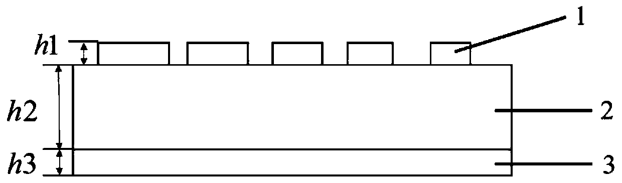
[0035] like figure 2 as shown, figure 2 It is the front view of the structure of the absorbing unit; in this embodiment, the material of the upper metal structure 1 is copper, and the electrical conductivity σ is set to 5.8×10 7 s / m, thickness h 1 set to 1 μm; the intermediate dielectric substrate layer 2 is made of polyimide 0, with a thickness of h 2 It is set to 50 μm; the reflective layer 3 of the lower metal base plate adopts a smooth copper plate as a substrate, and the thickness is h 3 If it is set to 20 μm, the reflective layer 3 of the lower metal base plate adopts a metal base, which can greatly reduce the transmission of electromagnetic waves, and the transmittance is negligible in simulation calculations.

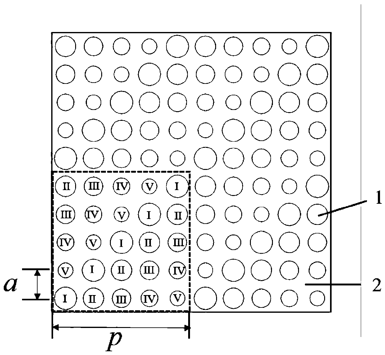
[0036] like image 3 as shown, image 3 It is a top view of the structure of the broadband metamaterial wave absorber; the metal discs with a radius of 80 μm to 120 μm and a thickness of 1 μm are periodically arranged on the intermediate dielectric substr...


PUM


Abstract

The invention discloses a broadband metamaterial wave-absorbing device. The broadband metamaterial wave-absorbing device comprises a plurality of wave-absorbing units extending in a plane mode, wherein each wave-absorbing unit comprises an upper metal resonance layer, a middle dielectric substrate layer and a lower metal bottom plate reflecting layer; the middle dielectric substrate layer is arranged between the upper metal resonance layer and the lower metal bottom plate reflecting layer; and the upper metal resonance layer comprises N2 metal wafers, wherein the metal wafers are periodicallyarranged on the middle dielectric substrate layer in an N*N mode so as to form a periodic array. The superposition of absorption peaks at different frequencies is realized by combining multiple metalswith different radiuses in the periodic array, so that the broadband absorption effect is achieved.

Description

technical field [0001] The invention relates to the technical field of electromagnetic wave absorption, in particular to a broadband metamaterial absorber. Background technique [0002] The absorbing structure is a type of functional material that effectively absorbs the electromagnetic waves projected onto its surface and significantly reduces the target echo intensity. Traditional absorbing materials such as ferrite, metal micropowder, silicon carbide, and conductive fibers are thick, heavy, and poor in stability. And other shortcomings, the scope of application is limited. The emergence of new metamaterial absorbing materials overcomes the thickness limitation brought by the diffraction effect to traditional absorbing materials, and has the advantages of thin thickness, light weight, and strong absorption. Metamaterials are artificial materials composed of subwavelength microstructure units arranged according to certain rules. The resonance properties of materials can b...

Claims


Application Information

Patent Timeline
Patent Type & Authority Applications(China)
IPC IPC(8): H01Q17/00H01Q15/00
Inventor 田丽华陈晨武帅
Owner CHINA ELECTRONIC TECH GRP CORP NO 38 RES INST
Why Eureka
Try Eureka