Processing method of binary transition metal oxide film nanometer patterns

A technology of oxide thin films and transition metals, applied in nanotechnology, nanotechnology, nanostructure manufacturing, etc., can solve problems such as probe physical damage

Inactive Publication Date: 2019-06-14
XIANGTAN UNIV
View PDF5 Cites 2 Cited by
  • Summary
  • Abstract
  • Description
  • Claims
  • Application Information

AI Technical Summary

Problems solved by technology

For example, Jin KonKim et al. used AFM probes to fabricate extremely high-density polymer nano-indentation arrays at room temperature (Naturenano

Method used


Image

  • Processing method of binary transition metal oxide film nanometer patterns
  • Processing method of binary transition metal oxide film nanometer patterns
  • Processing method of binary transition metal oxide film nanometer patterns

Examples


Embodiment 1

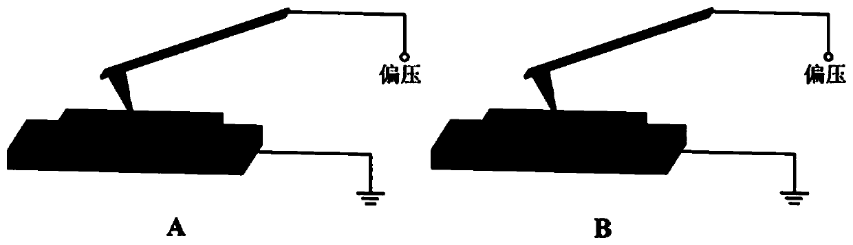
[0028] The first embodiment of the present invention is to perform single-point nanopattern processing on the binary transition metal oxide thin film under the condition of fixing the voltage amplitude applied by the probe. The schematic diagram of the processing is as follows figure 1 Shown in (A), its concrete mode of operation is:

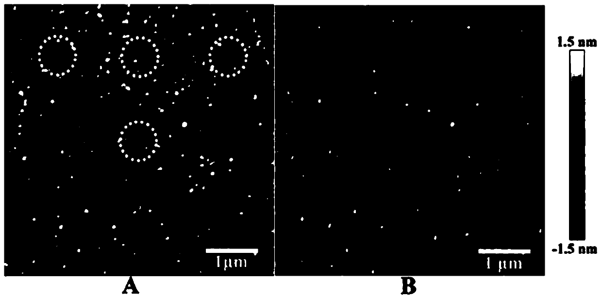
[0029] 1. If figure 2 As shown in (A), use the AFM tapping mode to scan a rectangular surface of 5 μm × 5 μm in the sample, and then select four points. The center position of the four white dotted circles is the position of the point where the probe tip contacts the sample during single-point processing.

[0030] 2. Switch the topography scanning mode of the C-AFM system to the contact mode.

[0031] 3. Accurately touch the probe tip to the selected four points, and apply a DC bias voltage of 0V-6V to the probe tip at the four points for 5, 20, 60, and 85 times respectively.

[0032] The following are the results of four specific processing...

Embodiment 2

[0039] The second embodiment of the present invention is to perform single-point nanopattern processing on the binary transition metal oxide thin film under the condition of fixing the number of voltages applied to the probe. The schematic diagram of the processing is as follows figure 1 Shown in (A), its concrete mode of operation is:

[0040] 1. If Figure 5 As shown in (A), use the AFM tapping mode to scan a rectangular surface of 10 μm × 10 μm in the sample, and then select three points. The position of the center of the three white dotted circles is the position of the point where the probe tip contacts the sample during single-point processing.

[0041] 2. Switch the topography scanning mode of the C-AFM system to the contact mode.

[0042] 3. Accurately touch the probe tip to the selected three points, and apply DC bias voltages of 0V-6V, 0V-8V, and 0V-10V respectively to the probe tip 50 times at the three points.

[0043] The following are the results of three spec...

Embodiment 3

[0048] The third embodiment of the present invention is to process nano-patterns of binary transition metal oxide films by scanning the surface of the powered probe, and the processing schematic diagram is as follows figure 1 Shown in (B), its specific mode of operation is:

[0049] 1. Use a C-AFM and apply a 10V DC bias to the probe tip.

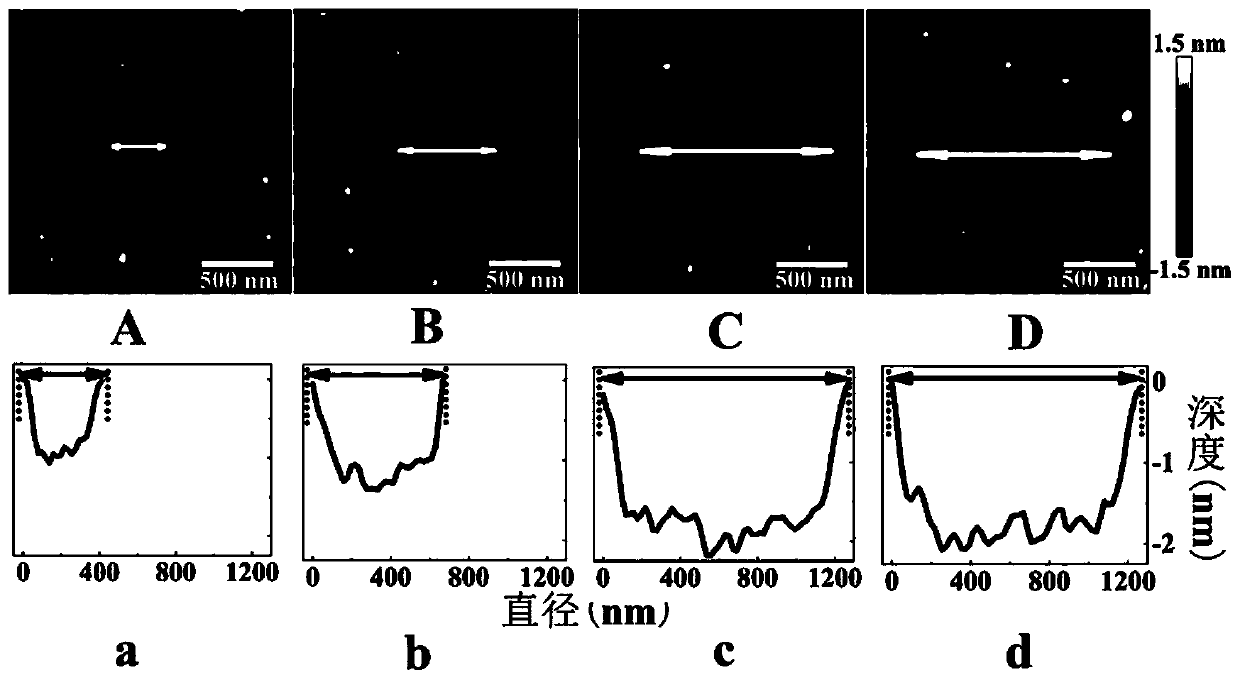
[0050] 2. If Figure 7 As shown, a rectangular area of ​​1 μm × 1 μm was scanned using the C-AFM contact mode, and the scanning times were 5 and 15 times, respectively.

[0051] The following are the results of two specific processing tests carried out using the method of this example:

[0052] Figure 8 The AFM topography diagrams of the circular nano-pits processed on the surface of the hafnium oxide film for the two specific processing tests of this embodiment and the corresponding diameter and depth diagrams of the circular nano-pits. Among them, the sub-graphs A and B are the AFM morphology of the circular nano-pits processed by sc...


PUM


Abstract

The invention discloses a processing method of binary transition metal oxide film nanometer patterns. According to the processing method, a conducting atomic force microscopy (C-AFM) probe needle point is applied with a certain direct current bias, so that ionic electrochemical reaction at the contact interface of a binary transition metal oxide film and the probe is realized, the amplitude value,applying times, needle point effect zone, and scanning times are controlled, so that processing of binary transition metal oxide film nanometer patterns of different shapes is realized. The processing method possesses following advantages: nanometer grade processing precision is achieved, processing process is simple and convenient, energy consumption is super low, no pollution is caused, and nomask is needed. The processing method is capable of reducing physical damage on probe needle point.

Description

technical field [0001] The invention discloses a nano-pattern processing method for a binary transition metal oxide thin film, which belongs to the field of micro-nano structure processing and relates to the field of nano-ionics. Background technique [0002] Micro-nano structure processing technology is a technology for processing fine structures at the micron scale and below, which was first applied to the preparation of integrated circuits. In recent years, the ever-developing micro-nano structure processing technology has been widely used in information storage, biology, aerospace and other fields. [0003] Traditional micro-nanostructure processing technologies include optical exposure technology, electron beam exposure technology, focused ion beam processing technology, laser processing technology, etc. However, the disadvantages of complex processing, expensive processing equipment, and micron-scale processing range limit the further development of micro-nanostructur...

Claims


Application Information

Patent Timeline
IPC IPC(8): B82B3/00B82Y40/00
Inventor 燕少安王冬龚俊王海龙
Owner XIANGTAN UNIV
Why Eureka
Try Eureka