Measuring method of grain layer thickness and judging method of grain layer abnormality

A thickness measurement and grain layer technology, applied in measurement devices, material analysis using measurement secondary emissions, and wave/particle radiation, etc. Reduce the discharge phenomenon, overcome the effect of easy charging and clear layer structure

Active Publication Date: 2021-04-02
SHENZHEN STS MICROELECTRONICS CO LTD
View PDF6 Cites 0 Cited by
  • Summary
  • Abstract
  • Description
  • Claims
  • Application Information

AI Technical Summary

Problems solved by technology

However, TEM machines are expensive and the sample preparation process is complicated, so it is impossible to quickly complete the analysis of the grain layer structure
[0008] Therefore, the current measurement methods for the grain layer structure of a single chip, or the grain layer structure in a finished product that has completed chip packaging, either have limited measurement accuracy, are expensive, and have a cumbersome measurement process, and cannot achieve fast, economical and accurate measurement. Purpose of Measuring Grain Layer Structure

Method used


Image

  • Measuring method of grain layer thickness and judging method of grain layer abnormality
  • Measuring method of grain layer thickness and judging method of grain layer abnormality
  • Measuring method of grain layer thickness and judging method of grain layer abnormality

Examples


Embodiment 1

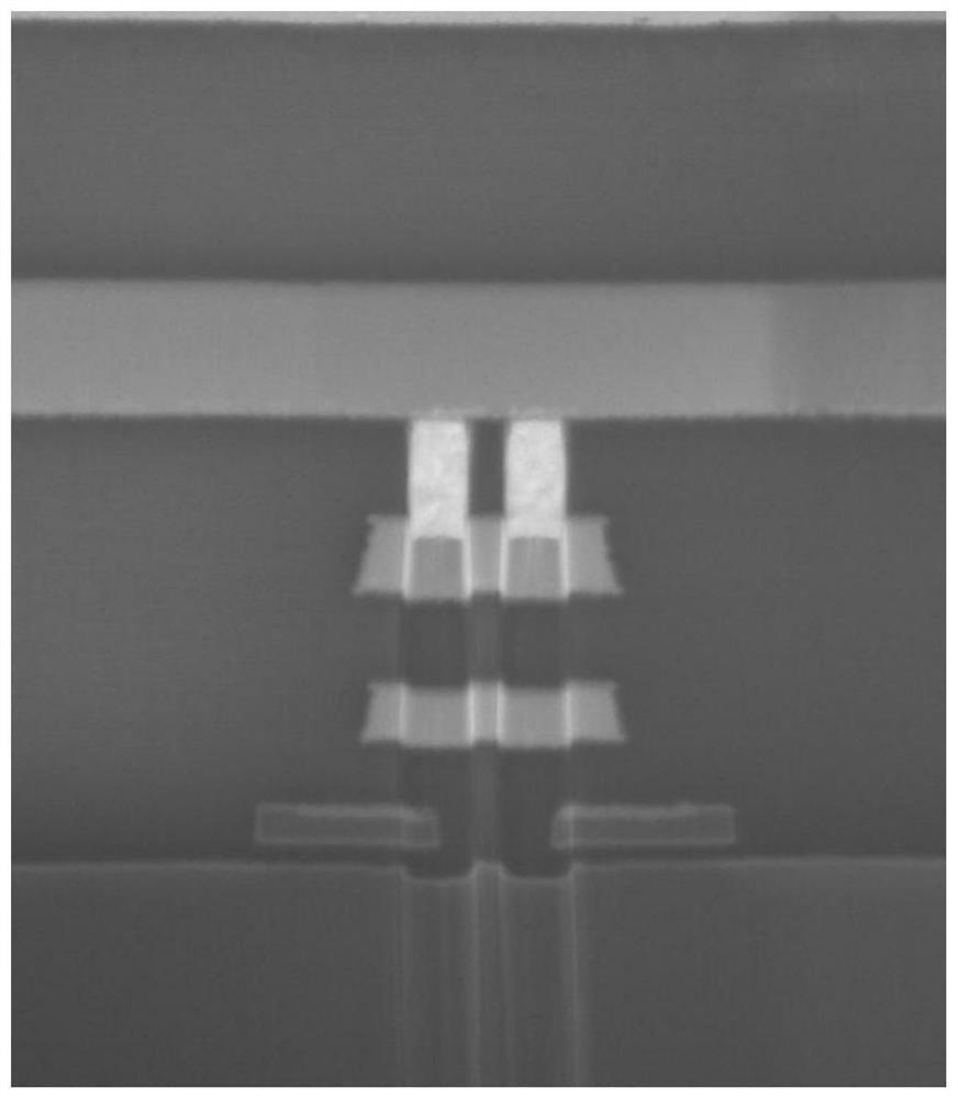
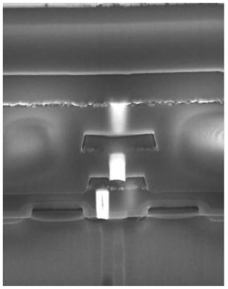
[0048] Such as Figure 2-6 As shown, the present invention provides a method for measuring the thickness of the grain layer. This embodiment is a method for measuring the thickness of each layer in a single grain layer structure, and the method at least includes the following steps:

[0049] Step S10: Process the grains to be tested to the target area using FIB;

[0050] Step S20: instill in the target area by CH 3 COOH, HNO 3 , HF or H 2 O, HNO 3 The mixed acid solution formed by mixing HF according to the preset ratio is cleaned after standing for a preset time, and the residual liquid of the crystal grains to be tested is removed to obtain the test sample;

[0051] Step S30: Using the SEM to observe and measure the test sample at a preset voltage.

[0052] In step S10, the sample to be tested is processed to a target area by using FIB, and the target area is the exposed area of ​​the grain to be tested after being treated by FIB, such as the area of ​​the longitudinal...

Embodiment 2

[0057] Such as Figure 7 As shown, the present invention also provides a method for measuring the thickness of the grain layer of a chip, including the method for measuring the thickness of the grain layer as provided in Example 1, and also includes a step before step S10: using a laser and / or a chemical unsealing method to remove the chip The packaging structure exposes the die inside the chip.

[0058] Specifically, the embodiment of the present invention can use the chemical unsealing method or the laser laser method to remove the packaging structure outside the chip. The first step is to remove the plastic package from the chip to be tested, so as to avoid damage to the grain layer structure of the chip by laser method alone. First use the laser method to remove most of the plastic packaging film of the chip to be tested, and then unpack it with chemicals to expose the internal crystal grains of the chip package. For chips soldered with gold wires, the chemical agent in ...

Embodiment 3

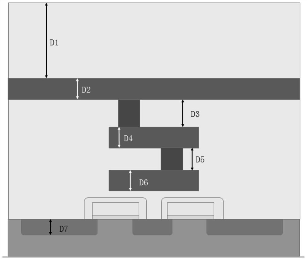
[0060] The invention also provides a method for judging the abnormality of the grain layer. The abnormality of the grain layer mainly means that the thickness of each structural layer in the grain layer deviates from the design standard value, which makes the grain have the risk of failure. The thickness of the grain layer is measured by the method provided in Embodiment 1 and compared with the standard value to determine whether there is an abnormality in the thickness of the grain and whether there is an abnormal layer. If it is within the standard value range, there is no abnormality in the grain layer; if the measured value of a certain layer in the grain layer, such as the measured value of D3 layer, exceeds the standard value range, it can be confirmed that there is an abnormality in the grain layer, and the abnormal position is at D3 layer. Wherein, the standard value may be a design standard value during design, or a standard reference value for a specific type of waf...


PUM


Abstract

The invention discloses a crystal particle layer thickness measuring method. The crystal particle layer thickness measuring method at least comprises the following steps that S10: FIB is used for treating to-be-tested crystal particles to a target area; S20: a mixed acid solution composed of mixed CH<3>COOH, HNO<3> and HF or H<2>O, HNO<3> and HF according to the preset proportion is dropwise addedinto the target area, still standing is conducted for preset time, then washing is conducted, liquid residues on the target area are removed, and a test sample is obtained; and S30: SEM is used for observing and measuring the test sample under a preset voltage. The invention further discloses a crystal particle layer abnormity judgement method, thicknesses of all layers in a crystal particle structure is measured through the crystal particle layer thickness measuring method and compared with standard values, whether abnormity exists in the thicknesses of the chip crystal particles or not is judged, and the abnormity exists in which layer is judged. The crystal particle layer thickness measuring method is used for overcoming the defect of a chip crystal particle layer thickness measuring method in the prior art, the operation is easy, and accuracy is high.

Description

technical field [0001] The invention relates to the technical field of semiconductor detection, in particular to a method for measuring the thickness of a chip grain layer and a method for judging abnormality of the grain layer. Background technique [0002] At present, with the rapid development of the performance and manufacturing technology of semiconductor integrated circuits and the need to reduce the cost of semiconductor integrated circuits, in the rapidly developing semiconductor industry, the analysis of chip layer structure plays an important role in the failure analysis of the internal grains of the chip. [0003] There are mainly three kinds of existing layer structure analysis methods: diamond knife fragmentation method, FIB (focused ion beam, FocusedIon beam) cutting analysis method, TEM (transmission electron microscope, Transmission electron microscope) analysis method. But they still have certain flaws: [0004] (1) The diamond fragmentation method can be u...

Claims


Application Information

Patent Timeline
Patent Type & Authority Patents(China)
IPC IPC(8): G01B15/02G01N23/22G01N23/2202
Inventor 龚瑜黄彩清吴凌
Owner SHENZHEN STS MICROELECTRONICS CO LTD
Why Eureka
Try Eureka