Coupling structure and packaging structure of laser and silicon light chip

A silicon photonic chip and packaging structure technology, applied in the direction of coupling of optical waveguides, can solve the problems of low chip reliability, affecting chip reliability, complex sealing process, etc. cost effect

Pending Publication Date: 2019-06-14
SUZHOU CREALIGHTS TECH
View PDF0 Cites 14 Cited by
  • Summary
  • Abstract
  • Description
  • Claims
  • Application Information

AI Technical Summary

Problems solved by technology

Among the above three schemes, the process of scheme 1 is complicated, the reliability of the chip is not high, and there is a lattice mismatch between the silicon material and the III-V semiconductor optoelectronic material itself. There will be many lattice defects, which will generate relatively large stress and affect the reliability of the chip; the processing technology of the light source component in the second scheme, the sealing process is more complicated, and the process cost is relatively high; the third scheme is to flip the laser chip waveguide on the silicon waveguide Above, evanescent wave coupling requires ultra-high-precision coupling and alignment equipment, which has high requirements for equipment and technology
To sum up, the existing technologies for realizing silicon light sources have certain defects, and there is a large room for improvement.

Method used


Image

  • Coupling structure and packaging structure of laser and silicon light chip
  • Coupling structure and packaging structure of laser and silicon light chip
  • Coupling structure and packaging structure of laser and silicon light chip

Examples


Embodiment Construction

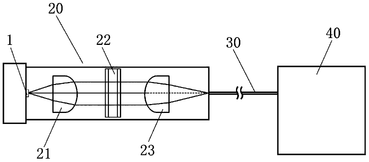
[0021] Such as figure 1 As shown, a coupling structure of a laser and a silicon photonics chip in the present invention includes a laser 1, a collimating lens 21, an isolator 22, a coupling lens 23, an optical fiber 30 and a silicon photonics chip 40 arranged in sequence. The collimating lens 21 and the coupling lens 23 have a common optical axis, the optical fiber 30 is connected to the silicon optical chip 40, the laser 1 emits a beam, and the beam and the collimating lens 21 have a common optical axis, and the incident beam The collimating lens 21, the light beam collimated by the collimating lens 21 enters the isolator 22, exits from the isolator 22, enters the coupling lens 23, and converges to the coupling lens 23 through the coupling lens 23. Fiber 30. The collimating lens 21 and the coupling lens 23 form a double-lens structure, and the coupling efficiency of the laser can be effectively improved after adopting this double-lens optical design. The silicon photonic ch...


PUM


Abstract

The invention discloses a coupling structure of a laser and a silicon optical chip. The coupling structure comprises a laser, a collimating lens, an isolator, a coupling lens, an optical fiber and thesilicon optical chip which are arranged in sequence; the collimating lens and the coupling lens share an optical axis; the optical fiber and the silicon optical chip are connected with each other; light emitted by the laser after passing through the collimating lens enters the isolator, then enters the coupling lens to be gathered at the optical fiber and finally enters the silicon optical chip through the optical fiber. The invention also discloses a packaging structure of the laser and the silicon optical chip. The packaging structure comprises a light emission assembly, the optical fiber and the silicon optical chip which are connected one by one; the light emission assembly comprises the laser, the collimating lens, the isolator and the coupling lens; the light emitting assembly is packaged by adopting a TOSA (Light Emission Module) technology; and the laser is packaged by adopting TO (Transistor Outline) technology.

Description

technical field [0001] The invention relates to the technical field of light-emitting communication, and more precisely relates to a coupling structure and packaging structure of a laser and a silicon optical chip. Background technique [0002] With the continuous development of optical communication technology, optoelectronic devices are developing in the direction of smaller size, higher integration and lower cost. Integrated circuit chips are generally manufactured on silicon chips using complementary metal-oxide-semiconductor integration technology, which already has a very mature manufacturing process. Now some manufacturers make waveguides on the side of silicon-based substrates for optical transmission, so that the functions of integrated circuit chips A silicon photonics chip is a silicon photonics chip that is integrated with the functions of an optical chip on the same silicon chip. Silicon photonic chips can not only realize electrical signal processing functions...

Claims


Application Information

Patent Timeline
Patent Type & Authority Applications(China)
IPC IPC(8): G02B6/42G02B6/32G02B6/27
Inventor 汪军平胡勇胡朝阳
Owner SUZHOU CREALIGHTS TECH
Why Eureka
Try Eureka