Resistive random access memory
A resistive variable memory and resistive variable technology, applied in the field of memory, can solve the problems of large fluctuation of resistive variable memory parameters, achieve the effects of reducing randomness, reducing current fluctuation, and improving reliability
- Summary
- Abstract
- Description
- Claims
- Application Information
AI Technical Summary
Problems solved by technology
Method used
Image
Examples
Embodiment 1
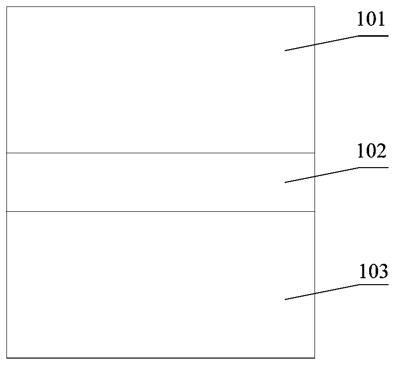
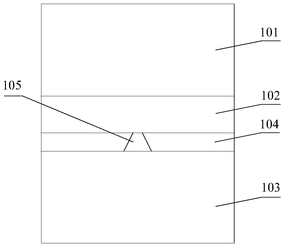
[0028] This embodiment provides a resistive random access memory, figure 2 It is a schematic diagram of the structure of the resistive random access memory. The resistive random access memory includes a first metal layer 101, a resistive function layer 102, a material layer 104 with low mobility, and a second metal layer 103 that are sequentially stacked from top to bottom, wherein the low mobility layer More than one through hole 105 is provided on the material layer 104.
[0029] Specifically, the first metal layer 101 serves as a metal upper electrode, which may be a platinum material layer or a gold material layer. Further, the thickness of the first metal layer 101 may be 50 nanometers to 100 nanometers.
[0030] The resistive function layer 102 is a binary transition metal oxide material layer, which can be a tantalum oxide material layer, a hafnium dioxide material layer, a titanium dioxide material layer, a nickel oxide material layer, or a zirconium dioxide material laye...
Embodiment 2
[0037] Based on the same inventive concept, this embodiment provides a method for manufacturing a resistive random access memory. Figure 5 It is a flow chart of the method for preparing the resistive random access memory. The method for preparing the resistive random access memory includes steps S11 to S16.
[0038] S11, provide a substrate.
[0039] In this embodiment, provide Figure 6a The glass substrate 100 is shown.
[0040] S12, depositing a first metal layer on the upper surface of the substrate.
[0041] Such as Figure 6b As shown, the first metal layer 101 is deposited on the upper surface of the glass substrate 100 by a deposition method such as magnetron sputtering, ion beam sputtering, or electron beam evaporation. The first metal layer 101 serves as a metal upper electrode, which may be a platinum material layer or a gold material layer. Further, the thickness of the first metal layer 101 may be 50 nanometers to 100 nanometers.
[0042] S13, depositing a resistive func...
PUM
| Property | Measurement | Unit |
|---|---|---|
| Thickness | aaaaa | aaaaa |
| Thickness | aaaaa | aaaaa |
| Thickness | aaaaa | aaaaa |
Abstract
Description
Claims
Application Information


