Method for preparing resistive random access memory

A resistive variable memory and resistive variable technology, applied in the field of memory, can solve the problems of large fluctuation of resistive variable memory parameters, and achieve the effect of reducing randomness, reducing current fluctuation, and simple preparation

Active Publication Date: 2019-06-21
INST OF MICROELECTRONICS CHINESE ACAD OF SCI
View PDF8 Cites 5 Cited by
  • Summary
  • Abstract
  • Description
  • Claims
  • Application Information

AI Technical Summary

Problems solved by technology

[0004] What the present invention aims to solve is the problem that the parameter fluctuation of the resistive variable memory is large

Method used


Image

  • Method for preparing resistive random access memory
  • Method for preparing resistive random access memory
  • Method for preparing resistive random access memory

Examples


Embodiment 1

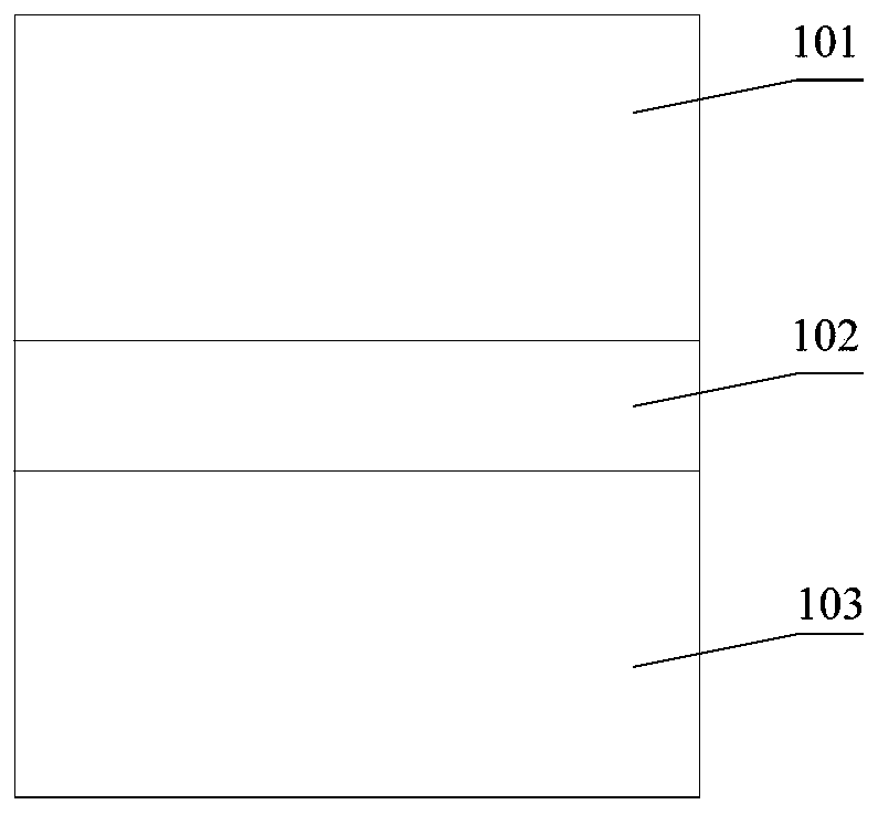
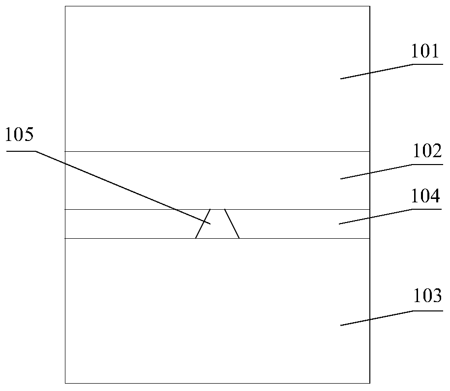
[0043] This embodiment provides a resistive variable memory, figure 2 is a structural schematic diagram of the resistive memory. The resistive switch memory includes a first metal layer 101, a resistive switch function layer 102, a material layer 104 with low mobility and a second metal layer 103 stacked sequentially from top to bottom, wherein the low mobility More than one through hole 105 is disposed on the material layer 104 .

[0044] Specifically, the first metal layer 101 serves as a metal upper electrode, which may be a platinum material layer or a gold material layer. Further, the thickness of the first metal layer 101 may be 50 nm to 100 nm.

[0045] The resistive switching function layer 102 is a binary transition metal oxide material layer, which may be a tantalum oxide material layer, a hafnium dioxide material layer, a titanium dioxide material layer, a nickel oxide material layer or a zirconium dioxide material layer. Further, the thickness of the resistive ...

Embodiment 2

[0052] Based on the same inventive concept, this embodiment provides a method for manufacturing a resistive variable memory. Figure 5 It is a flowchart of the preparation method of the resistive variable memory, and the preparation method of the resistive variable memory includes step S11 to step S16.

[0053] S11, providing a substrate.

[0054] In this example, provide Figure 6a A glass substrate 100 is shown.

[0055] S12, depositing a first metal layer on the upper surface of the substrate.

[0056] Such as Figure 6b As shown, the first metal layer 101 is deposited on the upper surface of the glass substrate 100 by magnetron sputtering, ion beam sputtering or electron beam evaporation and other deposition methods. The first metal layer 101 serves as a metal upper electrode, which may be a platinum material layer or a gold material layer. Further, the thickness of the first metal layer 101 may be 50 nm to 100 nm.

[0057] S13, depositing a resistive switching funct...


PUM

PropertyMeasurementUnit
thicknessaaaaaaaaaa
thicknessaaaaaaaaaa
thicknessaaaaaaaaaa

Abstract

The invention discloses a method for preparing a resistive random access memory. The method comprises the following steps of providing a substrate; depositing a first metal layer on the upper surfaceof the substrate; depositing a resistive functional layer on the upper surface of the first metal layer; depositing a material layer having a low mobility on the upper surface of the resistive functional layer; preparing one or more via holes on the material layer having the low mobility; and depositing a second metal layer on the upper surface of the material layer having the low mobility. According to the method for preparing a resistive random access memory provided by the invention, the resistive random access memory prepared can control the size of conductive filaments. Since the growth orientation, number and size of the conductive filaments can be controlled, the randomness of the growth of the conductive filaments can be reduced and the current fluctuation of the resistive random access memory can be reduced, thereby reducing the parameter fluctuation of the resistive random access memory and improving the reliability of the resistive random access memory.

Description

technical field [0001] The invention relates to the technical field of memory, in particular to a preparation method of a resistive variable memory. Background technique [0002] As a new type of non-volatile memory, RRAM (Resistive Random Access Memory) has the advantages of simple structure, fast working speed, low power consumption and stable information, and is a strong competitor of the next generation of non-volatile memory. one. figure 1 It is a structural diagram of an existing resistive memory, which includes a first metal layer 101, a resistive function layer 102, and a second metal layer 103 stacked sequentially from bottom to top. The working principle is: under the action of a positive electric field, the anode easily oxidizable metal of the second metal layer 103 as the upper electrode is oxidized into metal ions, and the metal ions pass through the resistive function layer 102 to the lower electrode. The first metal layer 101 moves and is reduced to metal at...

Claims


Application Information

Patent Timeline
Patent Type & Authority Applications(China)
IPC IPC(8): H01L45/00
Inventor 卢年端姜文峰李泠耿玓刘琦吕杭炳刘明
Owner INST OF MICROELECTRONICS CHINESE ACAD OF SCI
Why Eureka
Try Eureka