Fabrication process and application of a vertical-heterodomain organic spintronic device
A technology of spintronic devices and preparation process, applied in the field of spintronics, can solve problems such as uncontrollable effective length, low device repetition rate, complex interface, etc., and achieve the effect of avoiding electrical short circuit and avoiding electrical short circuit
- Summary
- Abstract
- Description
- Claims
- Application Information
AI Technical Summary
Problems solved by technology
Method used
Image
Examples
Embodiment 1
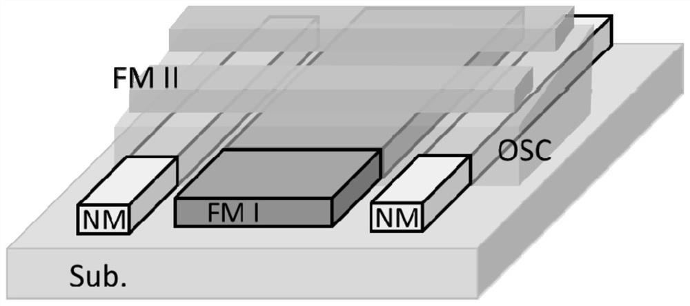
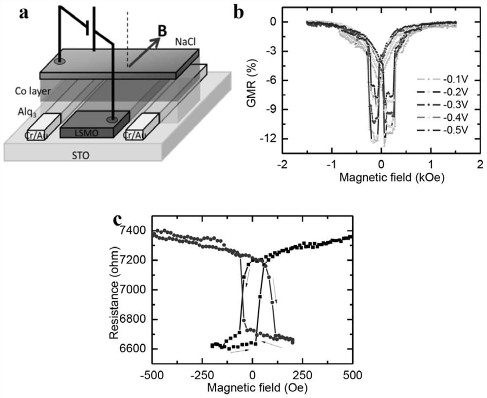
[0036] Using single crystal SrTiO 3 substrate, epitaxially grow a single crystal LSMO film with a thickness of 30nm on its surface, and optically etch it into a 50 micron wide strip electrode; then use the optical overlay method to grow Cr (5nm ) / Au(25nm) strip electrode; using ultra-high vacuum thermal evaporation to grow wedge-shaped organic layer Alq on the surface of LSMO and Cr / Au electrode 3 , the thickness of the wedge-shaped organic layer is 10-100nm, and the thickness of the wedge-shaped organic layer changes continuously along the direction of the LSMO strip electrode. The thinnest part is 10nm, and the thickest part is 100nm; A Co electrode with a thickness of 15nm is used, and a physical mask is used to realize the in-situ forming of the strip electrode. The direction is perpendicular to the LSMO electrode, and a NaCl protective layer is grown on the surface of the Co strip electrode.
[0037] The vertical-heterogeneous organic spintronic device prepared in this e...
Embodiment 2
[0040] Using single crystal SrTiO 3 substrate, epitaxially grow a single crystal LSMO film with a thickness of 30nm on its surface, and optically etch it into a 50 micron wide strip electrode; then use the optical overlay method to grow Cr (5nm ) / Au(25nm) strip electrode; using ultra-high vacuum thermal evaporation to grow wedge-shaped organic layer Alq on the surface of LSMO and Cr / Au electrode 3 , the thickness of the wedge-shaped organic layer is 10-100nm, and the thickness of the wedge-shaped organic layer changes continuously along the direction of the LSMO strip electrode. The thinnest part is 10nm, and the thickest part is 100nm; A Co electrode with a thickness of 15nm is used, and a physical mask is used to realize the in-situ forming of the strip electrode. The direction is perpendicular to the LSMO electrode, and a NaCl protective layer is grown on the surface of the Co strip electrode.
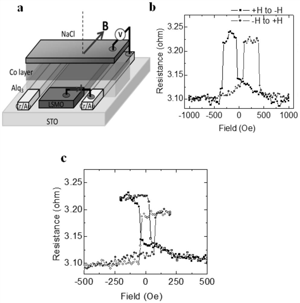
[0041] By applying a voltage between LSMO-Cr / Au, a spin-polarized current is i...
Embodiment 3
[0043] Using single crystal SrTiO 3 substrate, epitaxially grow a single crystal LSMO film with a thickness of 30nm on its surface, and optically etch it into a 50 micron wide strip electrode; then use the optical overlay method to grow Cr (5nm ) / Au(25nm) strip electrode; using ultra-high vacuum thermal evaporation to grow wedge-shaped organic layer Alq on the surface of LSMO and Cr / Au electrode 3 , the thickness of the wedge-shaped organic layer is 10-100nm, and the thickness of the wedge-shaped organic layer changes continuously along the direction of the LSMO strip electrode. The thinnest part is 10nm, and the thickest part is 100nm; A Co electrode with a thickness of 15nm is used, and a physical mask is used to realize the in-situ forming of the strip electrode. The direction is perpendicular to the LSMO electrode, and a NaCl protective layer is grown on the surface of the Co strip electrode.
[0044] By applying a voltage between LSMO-Cr / Au, a spin-polarized current is i...
PUM
| Property | Measurement | Unit |
|---|---|---|
| thickness | aaaaa | aaaaa |
| width | aaaaa | aaaaa |
| width | aaaaa | aaaaa |
Abstract
Description
Claims
Application Information


