Semiconductor device and method of forming the same

A semiconductor and device technology, applied in the field of semiconductor devices and their formation, can solve problems such as poor performance of semiconductor devices, achieve the effects of improving performance, avoiding impact, and reducing etching damage

Active Publication Date: 2022-03-22
SEMICON MFG INT (SHANGHAI) CORP +1
View PDF0 Cites 0 Cited by
  • Summary
  • Abstract
  • Description
  • Claims
  • Application Information

AI Technical Summary

Problems solved by technology

[0004] However, the performance of semiconductor devices composed of existing fin field effect transistors is poor

Method used


Image

  • Semiconductor device and method of forming the same
  • Semiconductor device and method of forming the same
  • Semiconductor device and method of forming the same

Examples


Embodiment Construction

[0030] As mentioned in the background, semiconductor devices formed in the prior art have poor performance.

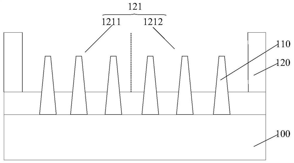
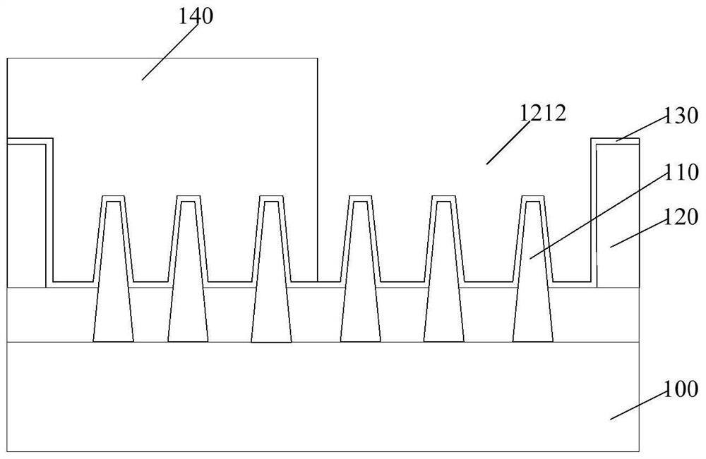
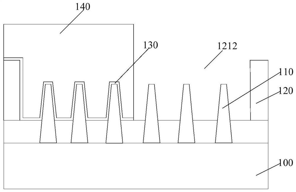
[0031] Figure 1 to Figure 4 It is a structural schematic diagram of the formation process of a semiconductor device.

[0032] refer to figure 1 , providing a semiconductor substrate 100 with a plurality of fins 110 on the semiconductor substrate 100; forming a dielectric layer 120 on the semiconductor substrate 100 and the fins 110; groove 121, the groove 121 includes a first groove region 1211 exposing part of the fin 110 and a second groove region 1212 exposing part of the fin 110, from the center of the first groove region 1211 to the center of the second groove region 1212 The direction is perpendicular to the extending direction of the fin portion 110 .

[0033] refer to figure 2 , form a gate dielectric layer (not shown) on the sidewalls and bottoms of the first groove region 1211 and the second groove region 1212 of the trench 121, a bottom work function l...


PUM

PropertyMeasurementUnit
thicknessaaaaaaaaaa
thicknessaaaaaaaaaa

Abstract

A semiconductor device and its forming method, wherein the method includes: forming a dielectric layer on a semiconductor substrate and a fin, the dielectric layer has a groove exposing the fin, and the groove includes a first groove region exposing part of the fin and the second groove area exposing part of the fin, the direction from the center of the first groove area to the center of the second groove area is perpendicular to the extending direction of the fin; forming a first work function layer on the fin at the bottom; forming a first covering layer in the first groove area of ​​the trench, the first covering layer being located on the first work function layer of the first groove area and exposing the second groove area The first work function layer of the second groove area is etched and removed with the first cover layer as a mask; after the first work function layer of the second groove area is etched and removed, the second groove of the trench A second covering layer is formed in the region; the second covering layer and the first covering layer are removed by etching. The method improves the performance of semiconductor devices.

Description

technical field [0001] The invention relates to the field of semiconductor manufacturing, in particular to a semiconductor device and a forming method thereof. Background technique [0002] MOS transistors are one of the most important components in modern integrated circuits. The basic structure of a MOS transistor includes: a semiconductor substrate; a gate structure located on the surface of the semiconductor substrate, a source region located in the semiconductor substrate on one side of the gate structure, and a drain region located in the semiconductor substrate on the other side of the gate structure. The working principle of the MOS transistor is: by applying a voltage to the gate structure, the current through the channel at the bottom of the gate structure is adjusted to generate a switching signal. [0003] With the development of semiconductor technology, the ability of the traditional planar MOS transistor to control the channel current becomes weaker, resultin...

Claims


Application Information

Patent Timeline
Patent Type & Authority Patents(China)
IPC IPC(8): H01L21/336H01L29/78
CPCH01L29/785H01L29/66795
Inventor 张城龙涂武涛王胜
Owner SEMICON MFG INT (SHANGHAI) CORP
Why Eureka
Try Eureka