Semiconductor device and manufacturing method thereof
A manufacturing method and semiconductor technology, applied in semiconductor devices, semiconductor/solid-state device manufacturing, electrical components, etc., can solve the problem of insufficient depletion, devices that cannot provide high-level breakdown voltage, and limited optimization of gate polycrystalline boundary electric field and other issues to achieve the effect of increasing the breakdown voltage
- Summary
- Abstract
- Description
- Claims
- Application Information
AI Technical Summary
Problems solved by technology
Method used
Image

Examples
preparation example Construction
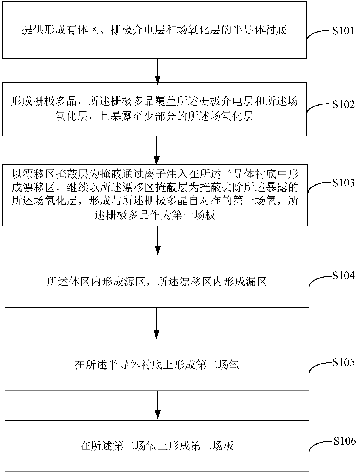
[0056] The invention provides a method for preparing a semiconductor device, such as figure 1 As shown, the main steps of the preparation method include:
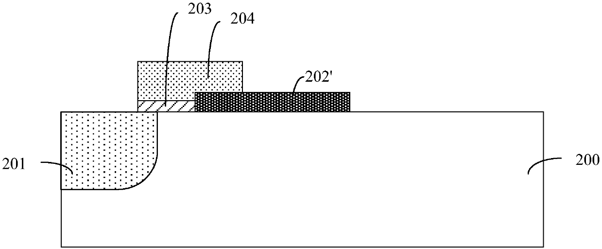
[0057] Step S101: providing a semiconductor substrate formed with a body region, a gate dielectric layer and a field oxide layer;
[0058] Step S102: forming a gate poly, the gate poly covers the gate dielectric layer and the field oxide layer, and exposes at least part of the field oxide layer;
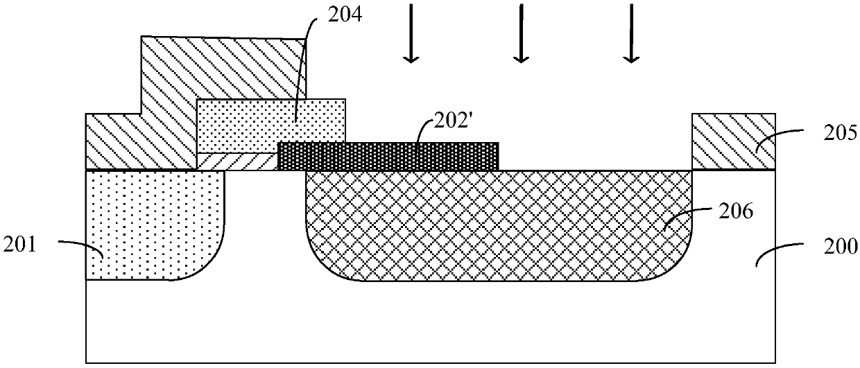
[0059] Step S103: using the drift region masking layer as a mask to form a drift region in the semiconductor substrate by ion implantation, continue to use the drift region masking layer as a mask to remove the exposed field oxide layer, and form a A first field oxygen of extremely polycrystalline self-alignment, the gate polycrystalline as a first field plate;
[0060] Step S104: forming a source region in the body region, and forming a drain region in the drift region;
[0061] Step S105: forming a second field oxygen on the ...
PUM
| Property | Measurement | Unit |
|---|---|---|
| Thickness | aaaaa | aaaaa |
| Thickness | aaaaa | aaaaa |
| Thickness | aaaaa | aaaaa |
Abstract
Description
Claims
Application Information
 - R&D
- Intellectual Property
- Life Sciences
- Materials
- Tech Scout
- Unparalleled Data Quality
- Higher Quality Content
- 60% Fewer Hallucinations
Browse by: Latest US Patents, China's latest patents, Technical Efficacy Thesaurus, Application Domain, Technology Topic, Popular Technical Reports.
© 2025 PatSnap. All rights reserved.Legal|Privacy policy|Modern Slavery Act Transparency Statement|Sitemap|About US| Contact US: help@patsnap.com