Packaging film, preparation method thereof, and photoelectric device
A technology for encapsulating films and composite films, which is applied in the field of device encapsulation, can solve problems such as poor bending resistance and water-oxygen barrier properties, and achieve the effects of improving water-oxygen barrier properties, reducing holes, and enhancing bonding properties
- Summary
- Abstract
- Description
- Claims
- Application Information
AI Technical Summary
Problems solved by technology
Method used
Image
Examples
Embodiment 1
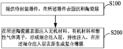
[0044] 1. The preparation method of encapsulation film comprises steps:
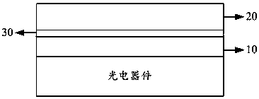
[0045] 1) On the top surface of the silver electrode of the photoelectric device, the aluminum nitride target is sputtered into a film by radio frequency sputtering, and the thickness of the aluminum nitride film is 50nm;
[0046] 2) Using the combination of inert gas ion implantation and sputtering, in the vacuum chamber, the vacuum degree is less than 10 -4 T, synchronously and uniformly implanting organic material PI, inorganic material silicon nitride and high-energy argon ions into the surface layer of the aluminum nitride film to form a mixed injection layer in the surface layer of the aluminum nitride film;
[0047] 3) When the mixed injection layer is sufficiently tight, a composite film is formed on the surface of the aluminum nitride film, and the thickness of the composite film is 150 nm.
Embodiment 2
[0049] 1. The preparation method of encapsulation film comprises steps:
[0050] 1) Evaporate silicon oxide to form a film on the top surface of the silver electrode of the photoelectric device by evaporation, and the thickness of the silicon oxide film is 100nm;
[0051] 2) Using the combination of inert gas ion implantation and sputtering, in the vacuum chamber, the vacuum degree is less than 10 -4 T, synchronously and uniformly implanting organic material PET, inorganic material silicon oxide, and high-energy argon ions into the surface layer of the silicon oxide film to form a mixed injection layer in the surface layer of the silicon oxide film;
[0052] 3) When the mixed injection layer is sufficiently tight, a composite film is formed on the surface of the silicon oxide film, and the thickness of the composite film is 200 nm.
Embodiment 3
[0054] 1. The preparation method of encapsulation film comprises steps:
[0055] 1) On the top surface of the silver electrode of the photoelectric device, silicon nitride is deposited into a film by ALD atomic deposition method, and the thickness of the silicon nitride film is 150nm;
[0056] 2) Using the combination of inert gas ion implantation and sputtering, in the vacuum chamber, the vacuum degree is less than 10 -4 T, synchronously and uniformly implanting organic material acrylic acid, inorganic material silicon nitride and high-energy argon ions into the surface layer of the silicon nitride film to form a mixed injection layer in the surface layer of the silicon nitride film;
[0057] 3) When the mixed injection layer is sufficiently dense, a composite film is formed on the surface of the silicon nitride film, and the thickness of the composite film is 300 nm.
[0058] In summary, the present invention provides packaging films, including laminated ceramic films and c...
PUM
| Property | Measurement | Unit |
|---|---|---|
| Thickness | aaaaa | aaaaa |
| Thickness | aaaaa | aaaaa |
| Thickness | aaaaa | aaaaa |
Abstract
Description
Claims
Application Information
 - R&D
- Intellectual Property
- Life Sciences
- Materials
- Tech Scout
- Unparalleled Data Quality
- Higher Quality Content
- 60% Fewer Hallucinations
Browse by: Latest US Patents, China's latest patents, Technical Efficacy Thesaurus, Application Domain, Technology Topic, Popular Technical Reports.
© 2025 PatSnap. All rights reserved.Legal|Privacy policy|Modern Slavery Act Transparency Statement|Sitemap|About US| Contact US: help@patsnap.com


