Electrostatic discharge protection structure and forming method and working method thereof
A technology of electrostatic discharge protection and gate structure, which is applied in the direction of circuits, electrical components, and electric solid devices, can solve the problems of poor performance of MOS tube electrostatic protection circuits, and achieve the effect of reducing the number of times and improving performance
- Summary
- Abstract
- Description
- Claims
- Application Information
AI Technical Summary
Problems solved by technology
Method used
Image

Examples
Embodiment Construction
[0027] As mentioned in the background, prior art ESD protection structures perform poorly.
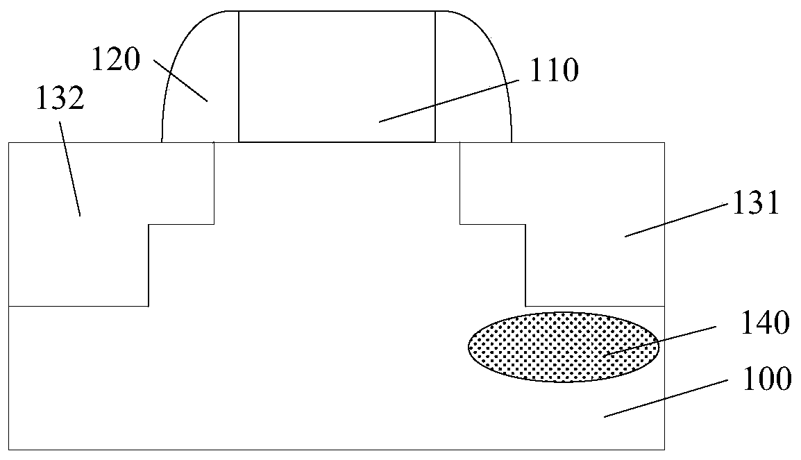
[0028] figure 1 It is a schematic diagram of the cross-sectional structure of an electrostatic discharge protection structure, please refer to figure 1 , the electrostatic discharge protection structure includes: a substrate 100, with a well region inside the substrate 100, the well region has first ions, and the concentration of the first ions is a first concentration; a gate structure located on the surface of the substrate 100 110; the drain doped region 131 and the source doped region 132 respectively located in the substrate 100 on both sides of the gate structure 110, the drain doped region 131 and the source doped region 132 contain second ions, the The conductivity type of the second ion is opposite to that of the first ion; the electrostatic protection doping region 140 located at the bottom of the drain doping region 131 has the first ions in the electrostatic protection dop...
PUM
 Abstract
Description
Claims
Application Information
 - R&D
- Intellectual Property
- Life Sciences
- Materials
- Tech Scout
- Unparalleled Data Quality
- Higher Quality Content
- 60% Fewer Hallucinations
Browse by: Latest US Patents, China's latest patents, Technical Efficacy Thesaurus, Application Domain, Technology Topic, Popular Technical Reports.
© 2025 PatSnap. All rights reserved.Legal|Privacy policy|Modern Slavery Act Transparency Statement|Sitemap|About US| Contact US: help@patsnap.com