Organic electroluminescence device and preparation method thereof

An electroluminescent device and electroluminescent technology, which are applied in the fields of organic semiconductor devices, electric solid state devices, chemical instruments and methods, etc., can solve the problems of high driving voltage and low exciton utilization efficiency, and achieve higher efficiency, higher energy and higher efficiency. Singlet excitons ratio, effect of increasing number

Active Publication Date: 2019-07-09
KUNSHAN GO VISIONOX OPTO ELECTRONICS CO LTD +1
View PDF10 Cites 12 Cited by
  • Summary
  • Abstract
  • Description
  • Claims
  • Application Information

AI Technical Summary

Problems solved by technology

[0006] Therefore, the technical problem to be solved by the present invention is to overcome the high driving voltage caused by the wide band gap of the host material of organic el...

Method used


Image

  • Organic electroluminescence device and preparation method thereof
  • Organic electroluminescence device and preparation method thereof
  • Organic electroluminescence device and preparation method thereof

Examples


Embodiment 1

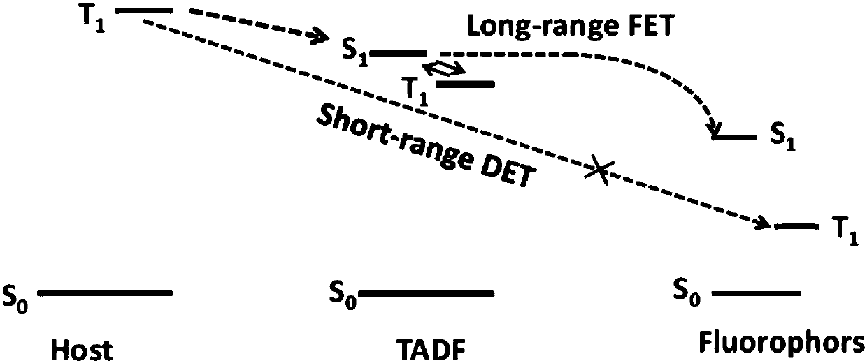
[0063] This embodiment provides an organic electroluminescence device, including a light-emitting layer, the light-emitting layer is formed by co-doping a host material, a TADF auxiliary host material, and a fluorescent dye, and the host material is formed by mixing an electron donor material and an electron acceptor material exciplexes.

[0064] Electron donor materials have the molecular structure shown below:

[0065]

[0066] Electron acceptor materials have the molecular structure shown below:

[0067]

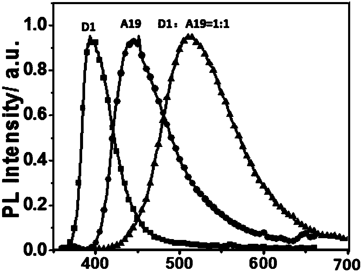
[0068] like figure 2 Compared with the emission spectra of the electron donor material and the electron acceptor material, the spectrum of the mixture of the electron donor material and the electron acceptor material is obviously red-shifted, indicating that the two form an exciplex.

[0069] TADF auxiliary host material (PXZ-DPS) has the molecular structure shown below:

[0070]

[0071] The fluorescent dye (YH201) has the molecular structure shown below:

...

Embodiment 2

[0080]This embodiment provides an organic electroluminescent device. The structure of the organic electroluminescent device is the same as that in Embodiment 1, except that the electron donor material of the formed exciplex has the structure shown in D2. The specific device structure is as follows The organic electroluminescent device forms the following specific structure: ITO / TAPC (30nm) / TCTA (10nm) / host (D2-A19 1:1):30wt%PXZ-DPS (TADF):3wt%YH201 (F) / Bphen (40nm ) / LiF(0.5nm) / Al(150nm).

[0081]

[0082]

Embodiment 3

[0084] This embodiment provides an organic electroluminescent device. The structure of the organic electroluminescent device is the same as that in Embodiment 1, except that the electron acceptor material of the formed exciplex has the structure shown in A35. The specific device structure is as follows The organic electroluminescent device forms the following specific structure: ITO / TAPC (30nm) / TCTA (10nm) / host (D1-A35 1:1): 30wt% PXZ-DPS (TADF): 3wt% YH201 (F) / Bphen (40nm ) / LiF(0.5nm) / Al(150nm).

[0085]


PUM


Abstract

The invention discloses an organic electroluminescence device. In a luminescent layer, a host material, an auxiliary host material and a fluorescent dye are contained; the host material is an exciplexformed by mixing an electron donor material and an electron acceptor material, the auxiliary host material is a thermally activated delayed fluorescent material, and a singlet-state energy level anda triplet-state energy level of the exciplex are respectively higher than those of the auxiliary host material. The organic electroluminescence device disclosed by the invention takes the exciplex with a narrow band gap as the host material, and the host material is codoped with a dye and an auxiliary host material with small DeltaEST, so that reverse intersystem crossing of the host material andthe auxiliary host material from a triplet-state excition to a singlet-state excition can be promoted, energy transmission is enhanced, quenching of the triplet-state excition is reduced, roll-off ofthe efficiency of the device is less, and the external quantum efficiency is high.

Description

technical field [0001] The invention belongs to the field of display technology, and in particular relates to an organic electroluminescent device and a preparation method thereof. Background technique [0002] As a new type of flat panel display technology, organic light emitting diodes (OLEDs, Organic Light Emitting Diods) mostly adopt a sandwich structure, that is, an organic light emitting layer is sandwiched between electrodes on both sides. Holes and electrons are injected from the anode and cathode respectively, and are transported in the organic layer to emit light. After meeting, the excitons are recombined to form excitons, and the excitons radiatively transition back to the ground state through the process of fluorescence or phosphorescence and emit light. Due to the advantages of wide viewing angle, ultra-thin, fast response, high luminous efficiency, and flexible display, OLED has great application prospects in the field of display and lighting, and has attracte...

Claims


Application Information

Patent Timeline
IPC IPC(8): H01L51/50H01L51/56H01L51/54
CPCH10K85/654H10K85/6572H10K50/12H10K71/00C09K11/06H10K85/615H10K85/631H10K85/657H10K50/11H10K2101/90H10K2101/20H10K85/40H10K85/322H10K85/622H10K85/623H10K85/624H10K85/633H10K85/653H10K50/15H10K50/16H10K50/81H10K50/82H10K2101/10
Inventor 段炼宋晓增张东东魏金贝
Owner KUNSHAN GO VISIONOX OPTO ELECTRONICS CO LTD
Why Eureka
Try Eureka