Hole material, OLED display panel containing same and electronic device
A technology for display panels and hole injection materials, applied in circuits, electrical components, electrical solid devices, etc., to achieve the effects of excellent electrochemical stability, high carrier transport rate, and high hole transport rate
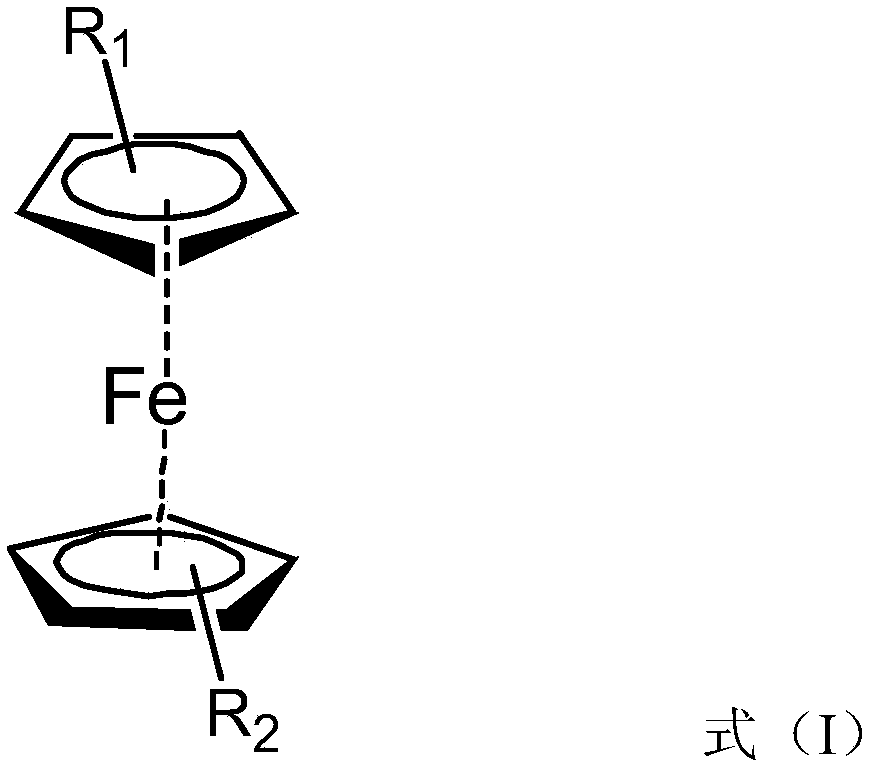
- Summary
- Abstract
- Description
- Claims
- Application Information
AI Technical Summary
Problems solved by technology
Method used
Image

Examples
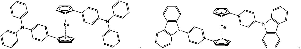
Embodiment 1
[0048] A compound HT1 A preparation method comprising the steps of:
[0049]
[0050] The synthesis conditions are:
[0051] In a 200mL two-necked bottle, add 1.38g bis-ferrocene boric acid, 4g anhydrous K 3 PO 4 powder, 3.5g bromotriphenylamine, 100mL anhydrous 1,4-dioxane, blow nitrogen for 30min, then add 0.15g Pd(PPh 3 ) 4 , Reflux reaction at 101°C for 24h in the dark. The device was cooled to room temperature, a large amount of water was added, and then the solid was filtered out, dried and recrystallized five times with 1,4-dioxane, and then sublimated to obtain 1.6 g of a tan solid (48% yield).
[0052] Characterization data:
[0053] Tg(DSC) 126°C, purity 99.9%;
[0054] 1 H NMR (400MHz, DMSO) δ7.23(d, 4H), 7.01(m, 8H), 6.62(d, 4H), 6.52(d, 4H), 6.46(m, 8H), 4.30(m, 4H) , 4.17(m,4H).
Embodiment 2
[0056] A compound HT2 A preparation method comprising the steps of:
[0057]
[0058] The synthesis conditions are the same as in Example 1, the yellowish brown solid has a yield of 43%.
[0059] Characterization data: Tg(DSC) 128°C, purity 99.9%;
[0060] 1 H NMR(400MHz,DMSO)δ7.55(d,4H),7.50(d,4H),7.40(d,4H),7.30(d,4H),7.08(m,4H),6.98(m,4H) ,4.27(m,4H),4.15(m,4H).
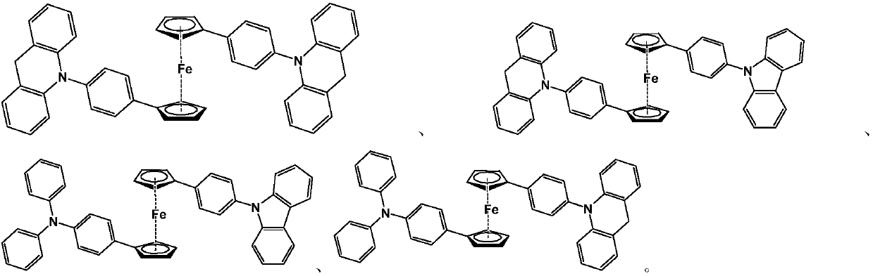
Embodiment 3
[0062] A compound HT3 A preparation method comprising the steps of:
[0063]
[0064] The synthesis conditions are the same as in Example 1, the yellowish brown solid has a yield of 45%.
[0065] Characterization data: Tg(DSC) 124°C, purity 99.9%;
[0066] 1 H NMR (400MHz,DMSO)δ7.23(d,4H),6.82-6.81(m,8H),6.52(d,4H),6.50(m,4H),6.34(d,4H),4.26(m, 4H), 4.13(m,4H), 3.80(s,4H).
PUM
 Abstract
Description
Claims
Application Information
 - R&D
- Intellectual Property
- Life Sciences
- Materials
- Tech Scout
- Unparalleled Data Quality
- Higher Quality Content
- 60% Fewer Hallucinations
Browse by: Latest US Patents, China's latest patents, Technical Efficacy Thesaurus, Application Domain, Technology Topic, Popular Technical Reports.
© 2025 PatSnap. All rights reserved.Legal|Privacy policy|Modern Slavery Act Transparency Statement|Sitemap|About US| Contact US: help@patsnap.com