Substrates for High Frequency Printed Wiring Boards
A printed circuit board and base material technology, which is applied in the fields of printed circuit, printed circuit, printed circuit manufacturing, etc., can solve the problems of low bonding strength between dielectric layer and copper foil, small surface energy of fluororesin, etc.
- Summary
- Abstract
- Description
- Claims
- Application Information
AI Technical Summary
Problems solved by technology
Method used
Image

Examples
no. 1 approach
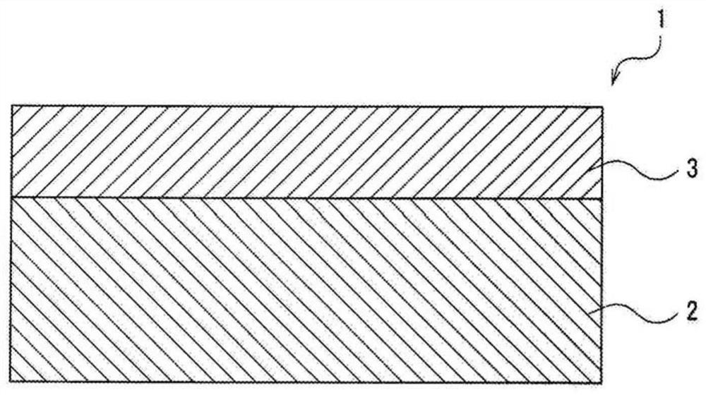
[0038] Such as figure 1 As shown, a base material 1 for a high-frequency printed wiring board according to the first embodiment includes a dielectric layer 2 and a copper foil 3 laminated on the dielectric layer 2 . This base material for a high-frequency printed wiring board is used as a base material of a printed wiring board.
[0039] (dielectric layer)
[0040] The dielectric layer 2 contains a fluororesin and an inorganic filler.
[0041](fluororesin)
[0042] The fluororesin refers to a resin in which at least one hydrogen atom bonded to a carbon atom contained in a repeating unit of a polymer chain is replaced by a fluorine atom or an organic group containing a fluorine atom (hereinafter, also referred to as "fluorine atom-containing group") substitution. The fluorine atom-containing group is a group in which a fluorine atom replaces at least one hydrogen atom in a linear or branched organic group. Examples of the fluorine atom-containing group include a fluoroalky...
no. 2 approach
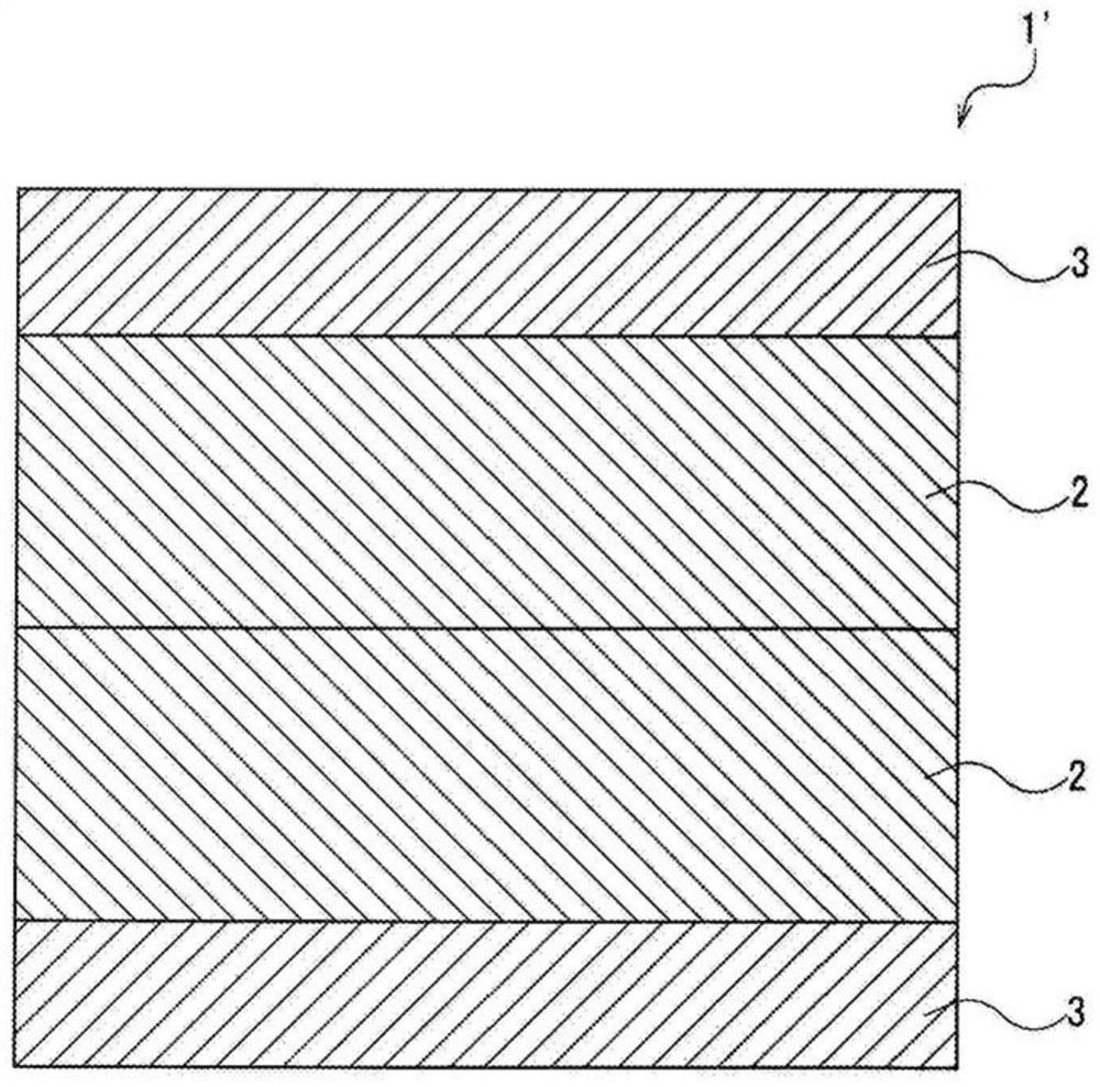
[0092] Such as figure 2 As shown, a base material 1' for a high-frequency printed wiring board according to the second embodiment includes: two dielectric layers 2 laminated on each other; and two copper foils 3 laminated on these dielectric layers 2, respectively. The base material 1' for a high-frequency printed wiring board generally has a structure in which two base materials 1 for a high-frequency printed wiring board are laminated|stacked on each other so that the side which opposes the copper foil 3 of each dielectric layer 2 faces each other.
[0093] In base material 1' for a high-frequency printed wiring board, dielectric layer 2 and copper foil 3 are the same as dielectric layer 2 and copper foil 3 in base material 1 for high-frequency printed wiring board, respectively.
no. 3 approach
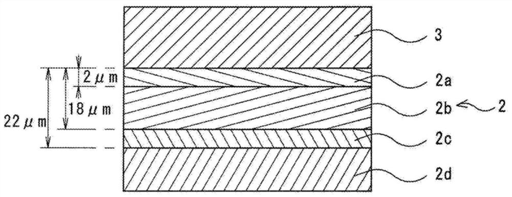
[0095] Such as Figure 4 As shown, a base material 1A for a high-frequency printed wiring board according to the third embodiment includes: a dielectric layer 2 including a layer 2A and a layer 2B; and a copper foil 3 laminated on the layer 2A. Layer 2A is a layer which contains a fluororesin and contains no inorganic filler or contains an inorganic filler in a content lower than that in layer 2B. Layer 2B is a layer containing a fluororesin and an inorganic filler.
[0096] In the base material 1A for a high-frequency printed wiring board, the layer 2B and the copper foil 3 are the same as the dielectric layer 2 and the copper foil 3 in the base material 1 for a high-frequency printed wiring board, respectively. When the dielectric layer 2 of the base material 1 for a high-frequency printed wiring board does not contain an inorganic filler, the layer 2A is the same as the dielectric layer 2 of the base material 1 .
PUM
| Property | Measurement | Unit |
|---|---|---|
| surface roughness | aaaaa | aaaaa |
| softening point | aaaaa | aaaaa |
| softening point | aaaaa | aaaaa |
Abstract
Description
Claims
Application Information
 - R&D
- Intellectual Property
- Life Sciences
- Materials
- Tech Scout
- Unparalleled Data Quality
- Higher Quality Content
- 60% Fewer Hallucinations
Browse by: Latest US Patents, China's latest patents, Technical Efficacy Thesaurus, Application Domain, Technology Topic, Popular Technical Reports.
© 2025 PatSnap. All rights reserved.Legal|Privacy policy|Modern Slavery Act Transparency Statement|Sitemap|About US| Contact US: help@patsnap.com