LED preparation method and LED
A light-emitting layer and electron technology, applied in electrical components, circuits, semiconductor devices, etc., can solve the problems of the effect of luminous efficiency, the reduction of the number and concentration of photons, the consumption of electrons and holes, etc. Effect of Luminous Efficiency
- Summary
- Abstract
- Description
- Claims
- Application Information
AI Technical Summary
Problems solved by technology
Method used
Image

Examples
Embodiment 1
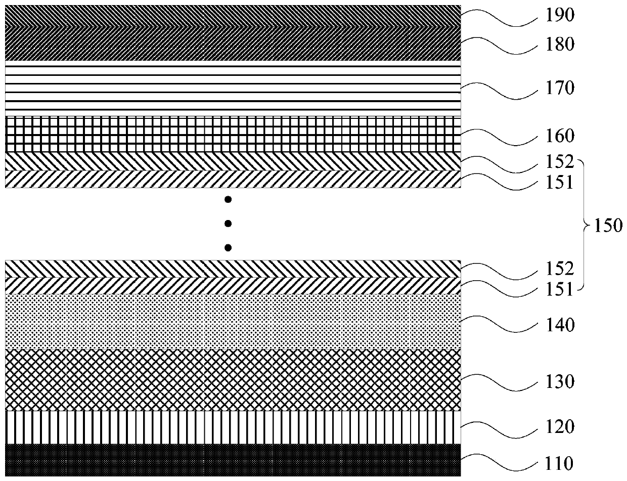
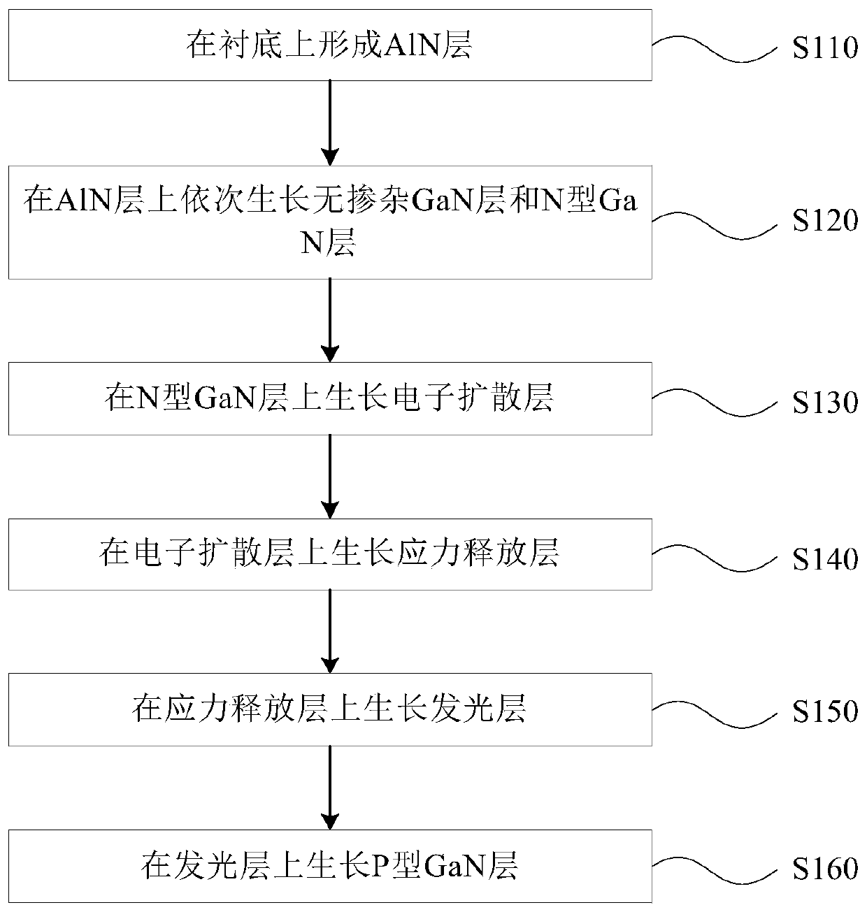
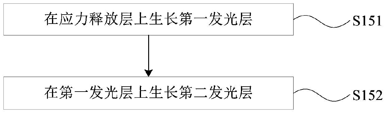
[0058] figure 2 It is a schematic flow chart of the LED manufacturing method provided by Embodiment 1 of the present invention. Such as figure 2 As shown, this embodiment provides a method for manufacturing an LED, comprising: forming an AlN layer on a substrate; growing an undoped GaN layer and an N-type GaN layer sequentially on the AlN layer; growing an electron diffusion layer on the N-type GaN layer ; growing a stress release layer on the electron diffusion layer; growing a light emitting layer on the stress release layer; growing a P-type GaN layer on the light emitting layer.
[0059] In this embodiment, GaN-based LEDs are grown on the substrate by MOCVD reaction. The substrate can be (0001) surface sapphire, and high-purity hydrogen, high-purity nitrogen, or a mixture of high-purity hydrogen and high-purity nitrogen can be used as the carrier gas , high-purity ammonia gas is used as the N source; in metal-organic sources, trimethylgallium (TMGa) and triethylgallium...
Embodiment 2
[0124] In this embodiment, the step S140 in the first embodiment: growing the stress release layer on the electron diffusion layer specifically includes the following steps:
[0125] Step c1: After S130, stop feeding metal-organic source and SiH 4 , maintain for 200-300 seconds, keep the pressure at 150-400 torr, continuously feed 30-300 liters / min of nitrogen as a carrier gas, continuously feed 30-200 liters / min of ammonia, reduce the temperature of the reaction chamber to 850 -950°C.
[0126] Step d1: maintain the reaction temperature at 850-950°C and the pressure at 100-300 torr, feed 30-300 liters / minute of nitrogen as a carrier gas for 300-400 seconds, and continuously feed 30-200 liters / minute of nitrogen at the same time Ammonia, 50-200 ml / min of the first gallium source and 2-10 ml / min of SiH at 200ppm 4 , grow a Si-doped N-type GaN layer with a thickness of 30-60nm on the electron diffusion layer, and the Si doping concentration is 1 E+18atoms / cm 2 -1E+19atoms / cm ...
Embodiment 3
[0135] In the LED manufacturing method provided in this embodiment, the above step S140 specifically includes the following steps:
[0136] Step c2: after S130, stop feeding metal-organic source and SiH 4 , maintained for 200 seconds, the pressure gradually changed from 150 torr to 250 torr, the continuous nitrogen gas was gradually changed from 50 liters / minute to 100 liters / minute, and the continuous ammonia gas was gradually changed from 60 liters / minute to 50 liters / min, the temperature of the reaction chamber gradually changes from 1000°C to 900°C.
[0137] Step d2: maintain the reaction temperature at 900°C and the pressure at 250 torr, and continue to feed 100 liters / minute of nitrogen as a carrier gas for 300 seconds, while continuously feeding 50 liters / minute of ammonia and 100 ml / minute of the first Gallium source and 6 mL / min of 200 ppm SiH 4 , grow a Si-doped N-type GaN layer with a thickness of 30-60nm on the electron diffusion layer, and the Si doping concent...
PUM
| Property | Measurement | Unit |
|---|---|---|
| Thickness | aaaaa | aaaaa |
| Thickness | aaaaa | aaaaa |
| Thickness | aaaaa | aaaaa |
Abstract
Description
Claims
Application Information
 - R&D
- Intellectual Property
- Life Sciences
- Materials
- Tech Scout
- Unparalleled Data Quality
- Higher Quality Content
- 60% Fewer Hallucinations
Browse by: Latest US Patents, China's latest patents, Technical Efficacy Thesaurus, Application Domain, Technology Topic, Popular Technical Reports.
© 2025 PatSnap. All rights reserved.Legal|Privacy policy|Modern Slavery Act Transparency Statement|Sitemap|About US| Contact US: help@patsnap.com