Method for detecting diffusion depth of semiconductor doping

A technology of diffusion depth and detection method, applied in the field of photodetectors, can solve the problem of difficulty in mass testing chips and low cost, and achieve the effect of real-time feedback and accurate test characterization

Active Publication Date: 2019-08-06
UNIV OF SCI & TECH OF CHINA
View PDF3 Cites 4 Cited by
  • Summary
  • Abstract
  • Description
  • Claims
  • Application Information

AI Technical Summary

Problems solved by technology

[0005] Aiming at the existing technical problems, the present invention proposes a method for detecting the diffusion depth of semiconductor doping, which is used to solve the problem that it is difficult to realize batch testing in the prior art, and is generally applicable to chips on the entire wafer, low cost, and non-destructive. Characterization detection problems of dopant diffusion

Method used


Image

  • Method for detecting diffusion depth of semiconductor doping
  • Method for detecting diffusion depth of semiconductor doping
  • Method for detecting diffusion depth of semiconductor doping

Examples


Embodiment Construction

[0031] In order to make the object, technical solution and advantages of the present invention clearer, the present invention will be described in further detail below in conjunction with specific embodiments and with reference to the accompanying drawings.

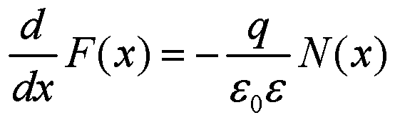
[0032] The present invention finds through research that for photodetectors based on P-N junction III-V semiconductor materials, the undoped region of the device is defined by using the epitaxial layer structure parameters, the lower edge of the cap layer and the diffusion edge, and then combines the gain and breakdown The voltage is a function of the thickness of the undoped part of the device region. It can be seen that the breakdown voltage and the diffusion depth satisfy the conditional equation of the Poisson equation in the physical model and the avalanche (that is, breakdown) in the impact ionization model, and the equation in the The unknown parameters are only the dopant diffusion thickness H and the breakdown vol...


PUM


Abstract

The invention relates to a method for detecting the diffusion depth of semiconductor doping, which comprises the steps of conducting diffusion of a doping agent, and measuring breakdown voltage of a semiconductor photoelectric detection device; calculating the diffusion depth of the doping agent according to the breakdown voltage, and carrying out supplementary diffusion on the device according tothe detected diffusion depth so as to optimize the diffusion process. The detection method does not need to complete tape-out proceses of all chips or split the chips into single chip devices, and does not need destructive sample preparation of other characterization detection means. In addition, the method can carry out large-scale fast and nondestructive testing and sampling on dots on siliconwafers while completing the diffusion of the doping agent, and is accurate, efficient and nondestructive in test characterization. The diffusion process is optimized based on the method so as to achieve expected objectives and subsequent tape-out processes.

Description

technical field [0001] The invention relates to the field of photodetectors, in particular to a method for detecting the diffusion depth of semiconductor doping. Background technique [0002] The thermal diffusion of semiconductor dopants is often used in III-V semiconductor photodetectors based on P-N junctions. Metal-organic Chemical Vapor Deposition (MOCVD), the diffusion profile and depth, etc. The gas flow rate, temperature, carrier gas flow rate, time and other parameters are related, and the diffusion process of III-V semiconductor photodetector chips based on P-N junctions often requires multiple diffusions, and each diffusion is not uniformly diffused across the entire chip. There are different situations such as forward diffusion, lateral diffusion, and constant concentration diffusion. It needs to be analyzed with the help of various advanced characterization methods. [0003] At present, the characterization and detection methods commonly used for the diffusion...

Claims


Application Information

Patent Timeline
Patent Type & Authority Applications(China)
IPC IPC(8): H01L21/66
CPCH01L22/14H01L22/20
Inventor 王亮张博健秦金
Owner UNIV OF SCI & TECH OF CHINA
Why Eureka
Try Eureka