

GaN heterojunction field effect transistor with high frequency and low junction temperature
A heterojunction field effect, low junction temperature technology, applied in the direction of transistors, semiconductor devices, electrical components, etc., can solve the problem of limiting the operating frequency of AlGaN/GaN heterojunction field effect transistors, damaging the connecting die wires, and accelerating electromigration and other issues, to achieve the effect of optimizing gate Schottky leakage characteristics, accelerating heat dissipation, and reducing channel temperature
Inactive Publication Date: 2019-08-09
UNIV OF ELECTRONICS SCI & TECH OF CHINA
View PDF6 Cites 2 Cited by
- Summary
- Abstract
- Description
- Claims
- Application Information
AI Technical Summary
Problems solved by technology
When the device works in a high voltage and short channel state, the material will produce a reverse piezoelectric polarization effect due to an excessively strong electric field, thereby degrading the material, and in severe cases, it will produce microcracks in the material. Therefore, AlGaN is used as the When the barrier layer is used, its material properties limit the further improvement of the operating frequency of AlGaN / GaN heterojunction field effect transistors
[0008] 2. Self-heating effect
Self-heating effects can accelerate electromigration, degrade the gate, and can damage the wires connecting the die to the package case, causing a series of reliability problems
Method used
View moreImage
Smart ImageViewing Examples

Examples
Embodiment Construction
[0032] The solution in the summary of the invention is the best implementation solution of the present invention, and will not be repeated here.
Login to View More PUM
 Abstract
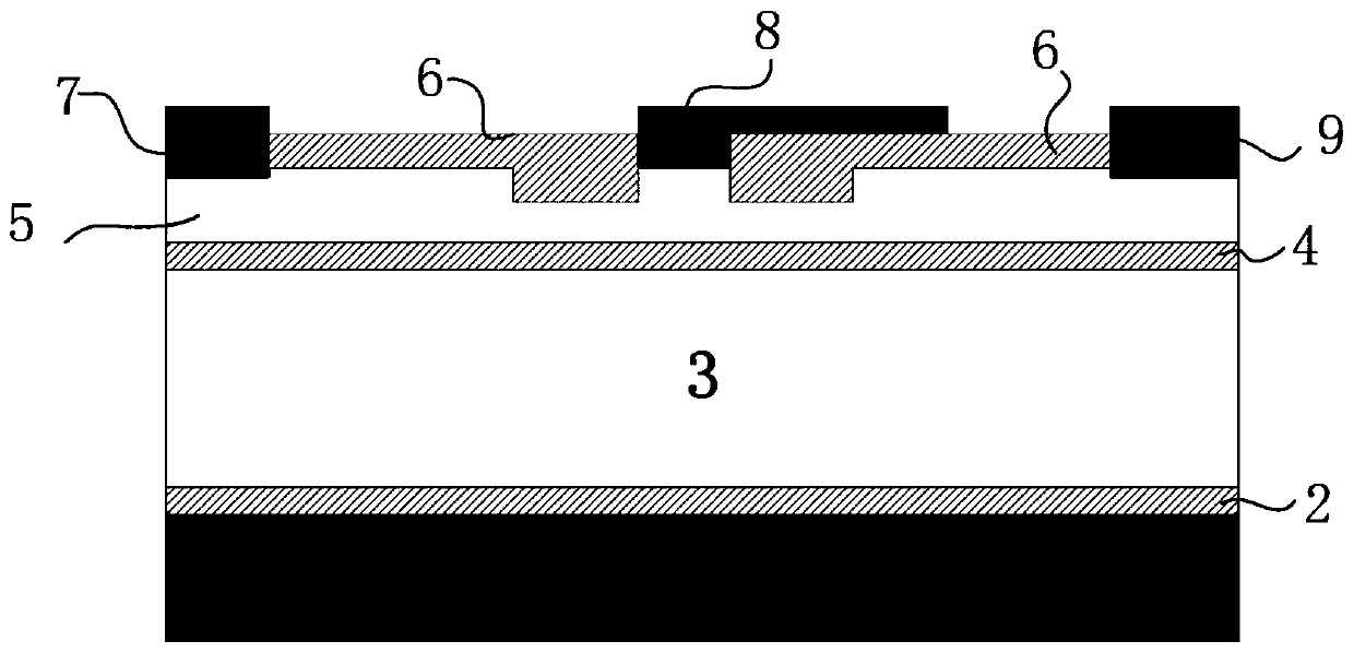
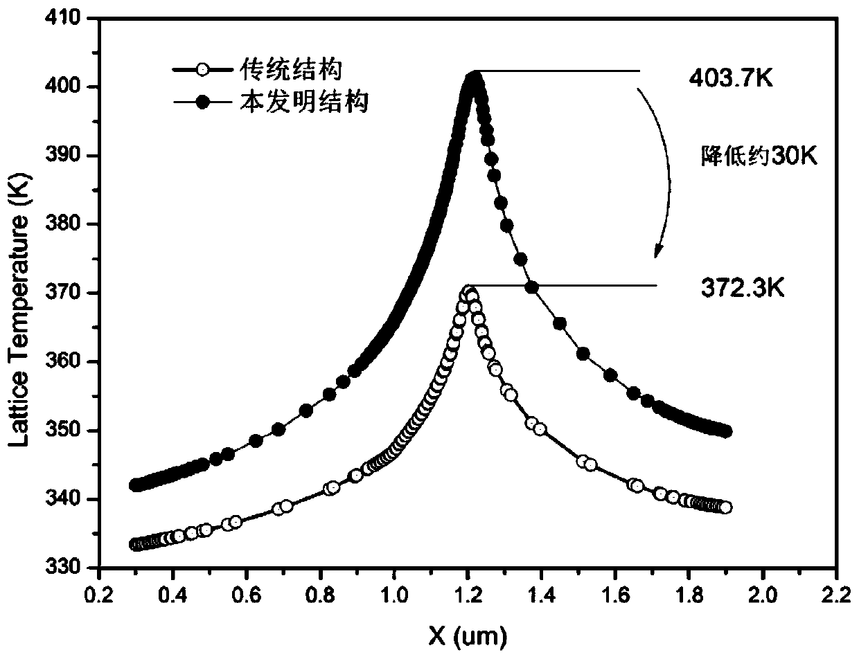
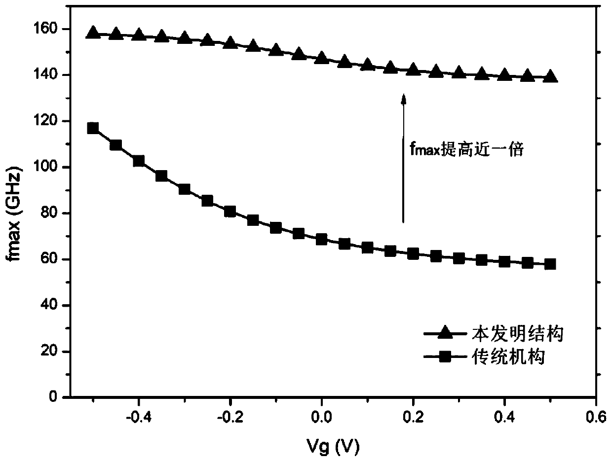
The invention relates to the technical field of power semiconductors, in particular to a GaN heterojunction field effect transistor with a high frequency and a low junction temperature. The GaN heterojunction field effect transistor mainly takes an InAlN as the barrier layer material of a device, the reverse piezoelectric effect is avoided when the InAlN and GaN form a heterojunction so as to overcome the defects that AlGaN is used as the barrier layer material in a traditional structure and facilitate improvement of the working frequency of the device. Besides, the barrier layer employs a biconcave structure, the two sides of a gate are both provided with grooves to improve the electric field distribution condition of a channel, improve the device voltage withstand and reduce the heat generation of the device channel. The channel temperature of the device is reduced, the bad influence of a 'self-heating effect' on the device is weakened, and the working frequency of the device is improved. The GaN heterojunction field effect transistor is especially suitable for the GaN heterojunction field effect transistor with a high frequency and a low channel temperature.
Description
technical field [0001] The invention belongs to the technical field of power semiconductors and relates to a GaN heterojunction field effect transistor with high frequency and low junction temperature. Background technique [0002] With the advancement of science and technology, the demand for electric energy in human society is increasing day by day. How to efficiently use electric energy has become a problem that has to be considered at present. At present, almost all electrical energy must be converted by power semiconductor devices before it can be used by electronic equipment. As one of the foundation and core technologies of new energy and energy conservation and emission reduction, power semiconductor technology has effectively promoted the application of electric energy in a more efficient, energy-saving and environmentally friendly manner. In recent years, with the rise of new energy vehicles and other fields, power semiconductor technology has a broader applicatio...
Claims
Login to View More Application Information
Patent Timeline
 Patent Type & AuthorityApplications(China)
IPC IPC(8): H01L29/06H01L29/10H01L29/20H01L29/47H01L29/778
CPCH01L29/0611H01L29/1029H01L29/2003H01L29/475H01L29/778
Inventor陈万军李佳刘熙信亚杰孙瑞泽
OwnerUNIV OF ELECTRONICS SCI & TECH OF CHINA