A kind of accumulation type MOS varactor diode based on tsv and its preparation method

A varactor, accumulation-type technology, used in semiconductor/solid-state device manufacturing, advanced technology, climate sustainability, etc., can solve problems such as large signal loss, and achieve high quality factor, no signal loss, and low parasitic resistance. Effect

Active Publication Date: 2022-05-20
XIAN UNIV OF TECH
View PDF4 Cites 0 Cited by
  • Summary
  • Abstract
  • Description
  • Claims
  • Application Information

AI Technical Summary

Problems solved by technology

[0005] An object of the present invention is to provide a TSV-based accumulation type MOS varactor diode, which solves the problem of large signal loss caused when the existing planar accumulation type varactor is applied to a three-dimensional integrated circuit and a three-dimensional adapter board

Method used


Image

  • A kind of accumulation type MOS varactor diode based on tsv and its preparation method
  • A kind of accumulation type MOS varactor diode based on tsv and its preparation method
  • A kind of accumulation type MOS varactor diode based on tsv and its preparation method

Examples


preparation example Construction

[0033] A kind of preparation method of the accumulation type MOS varactor diode based on TSV of the present invention, comprises the following steps:

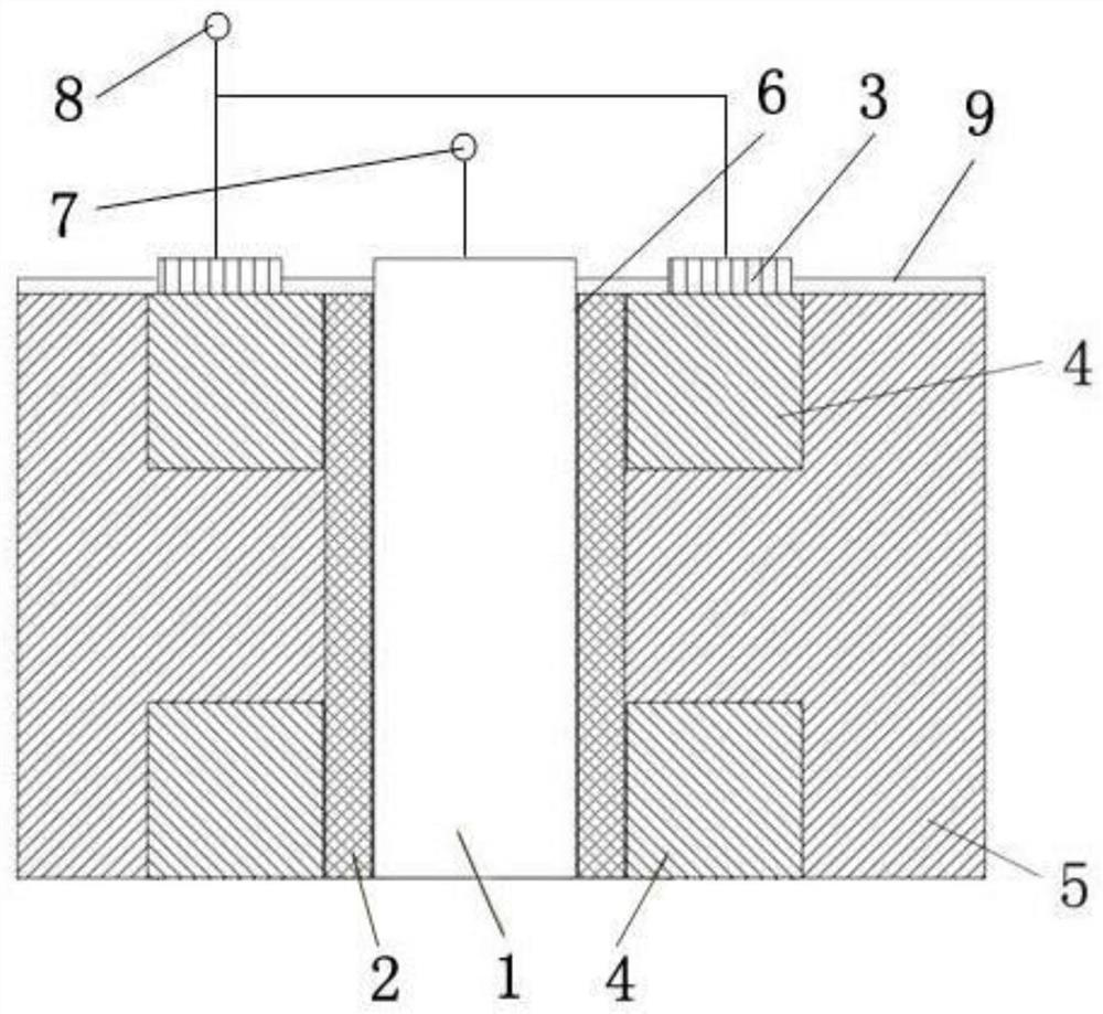
[0034] Step 1: Etch vertical through-holes 6 on the P-type silicon substrate 5 by means of reactive ions; use fluoride or chloride reactive gases to decompose fluorine atoms or chlorine atoms in glow discharge, and connect with the silicon substrate The silicon atoms on the surface of the bottom 5 react to form gaseous products to complete the etching of the vertical through hole 6; the pressure of the reaction gas is 14-31Pa, the flow rate of the reaction gas is 11-42 ml / min, and the radio frequency power range is 210-360W; During the process, heat exchangers and helium cooling technology are used to control the temperature of the silicon substrate to ensure that the temperature of the entire silicon substrate 5 during the etching process is uniform and stable at about 145°C.

[0035] Step 2, prepare the dielectric layer 2 on ...

Embodiment 1

[0041] The preparation of a TSV-based accumulation MOS varactor diode specifically includes the following steps:

[0042] Step 1: Etch vertical through-holes 6 on the P-type silicon substrate 5 by means of reactive ions; use chloride reactive gas to decompose chlorine atoms in glow discharge, and silicon atoms on the surface of the silicon substrate 5 The reaction generates gaseous products to complete the etching of the vertical through hole 6; the reaction gas pressure is 14Pa, the reaction gas flow rate is 16 ml / min, and the radio frequency power range is 260W; during the etching process, heat exchanger and helium cooling technology are used Control the temperature of the silicon substrate to ensure that the temperature of the entire silicon substrate 5 during the etching process is uniform and stable at about 145°C;

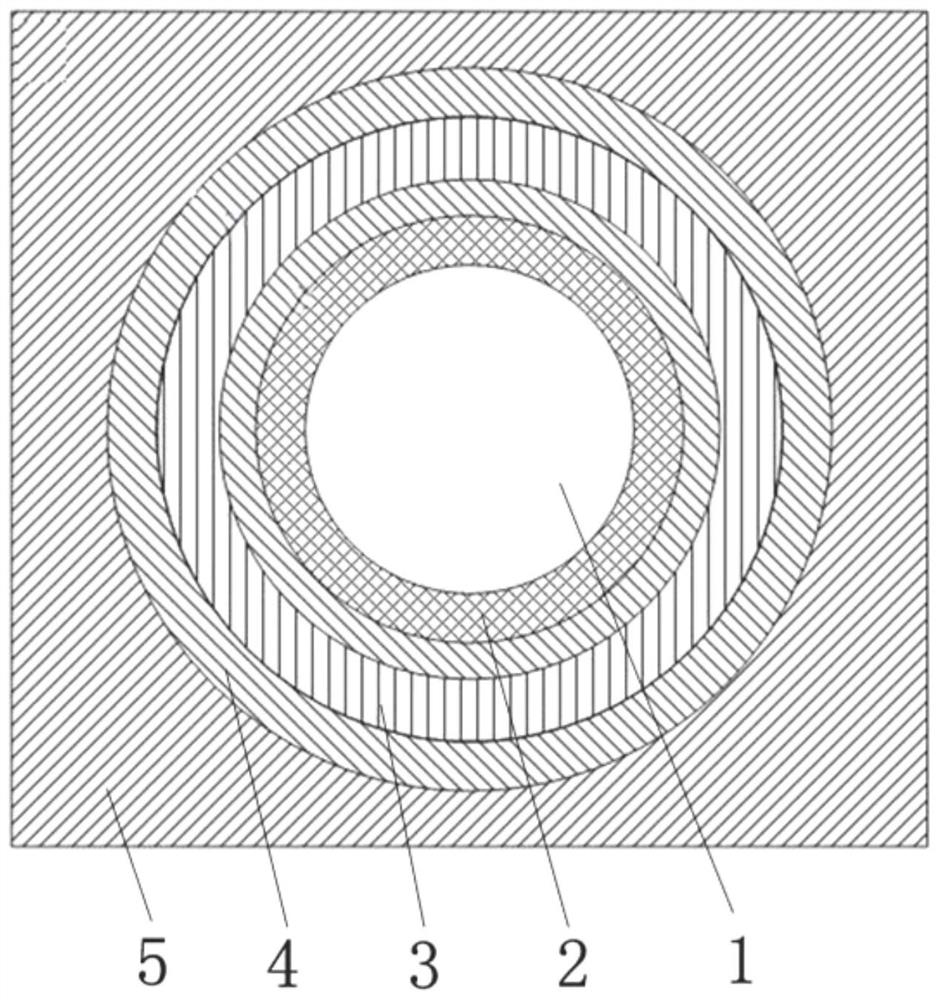
[0043] Step 2, on the inner wall of the through hole 6, the annular dielectric layer 2 is prepared by the atmospheric pressure chemical vapor deposition meth...

Embodiment 2

[0050] The preparation of a TSV-based accumulation MOS varactor diode specifically includes the following steps:

[0051] Step 1: Etch vertical through holes 6 on the P-type silicon substrate 5 by means of reactive ions; use fluoride reactive gas to decompose fluorine atoms in the glow discharge, and the silicon atoms on the surface of the silicon substrate 5 The reaction generates gaseous products to complete the etching of the vertical through hole 6; the reaction gas pressure is 24Pa, the reaction gas flow rate is 20 ml / min, and the radio frequency power range is 300W; during the etching process, heat exchangers and helium cooling technology are used Control the temperature of the silicon substrate to ensure that the temperature of the entire silicon substrate 5 during the etching process is uniform and stable at about 145°C;

[0052] Step 2, on the inner wall of the through hole 6, the annular dielectric layer 2 is prepared by the atmospheric pressure chemical vapor deposi...


PUM


Abstract

The invention discloses a TSV-based accumulation type MOS varactor diode, which includes a P-type silicon substrate, and a through hole is opened on the silicon substrate, and a metal column and a dielectric layer are sequentially arranged in the through hole from the inside to the outside, and the metal column leads out There is a terminal a, a P-type doped region is set between the dielectric layer near the end of the through hole and the silicon substrate, and a terminal b is drawn out from the end surface of the P-type doped region. The invention also discloses a preparation method of the accumulation type MOS varactor diode based on TSV. Compared with the planar accumulation type MOS varactor diode, the accumulation type MOS varactor diode of the present invention has higher quality factor and lower Parasitic resistance, lower phase noise and better tuning linearity.

Description

technical field [0001] The invention belongs to the technical field of three-dimensional integrated circuits, and in particular relates to a TSV-based cumulative MOS varactor diode and a preparation method thereof. Background technique [0002] With the advent of the 4G era, wireless communication technology has developed rapidly. Voltage Controlled Oscillator (VCO) is one of the core modules in wireless communication radio frequency system, and its research has attracted extensive attention. Because the CV characteristics and QV characteristics of the varactor diode have a huge impact on the VCO circuit, it has become one of the core devices of the VCO circuit. [0003] Traditional VCO circuits mostly use reverse-biased varactor diodes as voltage-controlled devices, but when implementing circuits with actual processes, varactor diodes usually have a small quality factor, narrow capacitance variable range, and limited control voltage. Factors that affect circuit performanc...

Claims


Application Information

Patent Timeline
Patent Type & Authority Patents(China)
IPC IPC(8): H01L29/93H01L29/94H01L21/329
CPCH01L29/93H01L29/94H01L29/66181Y02D30/70
Inventor 王凤娟文炳成余宁梅
Owner XIAN UNIV OF TECH
Why Eureka
Try Eureka