Semiconductor device and method of forming the same

A semiconductor and device technology, applied in the field of semiconductor devices and their formation, can solve problems such as poor performance of semiconductor devices

Active Publication Date: 2021-03-09
SEMICON MFG INT (SHANGHAI) CORP +1
View PDF7 Cites 0 Cited by
  • Summary
  • Abstract
  • Description
  • Claims
  • Application Information

AI Technical Summary

Problems solved by technology

[0004] However, the performance of semiconductor devices formed by prior art is poor

Method used


Image

  • Semiconductor device and method of forming the same
  • Semiconductor device and method of forming the same
  • Semiconductor device and method of forming the same

Examples


Embodiment Construction

[0031] As mentioned in the background, semiconductor devices formed in the prior art have poor performance.

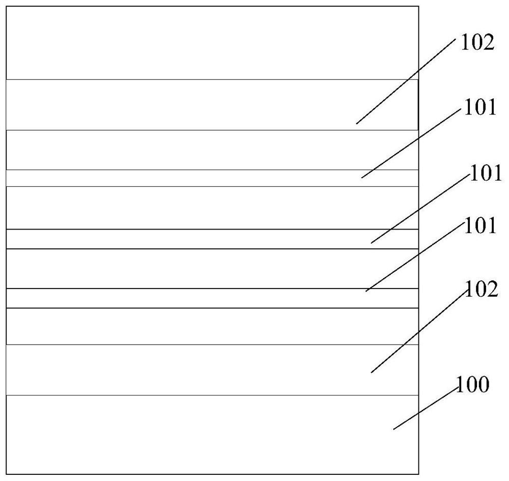
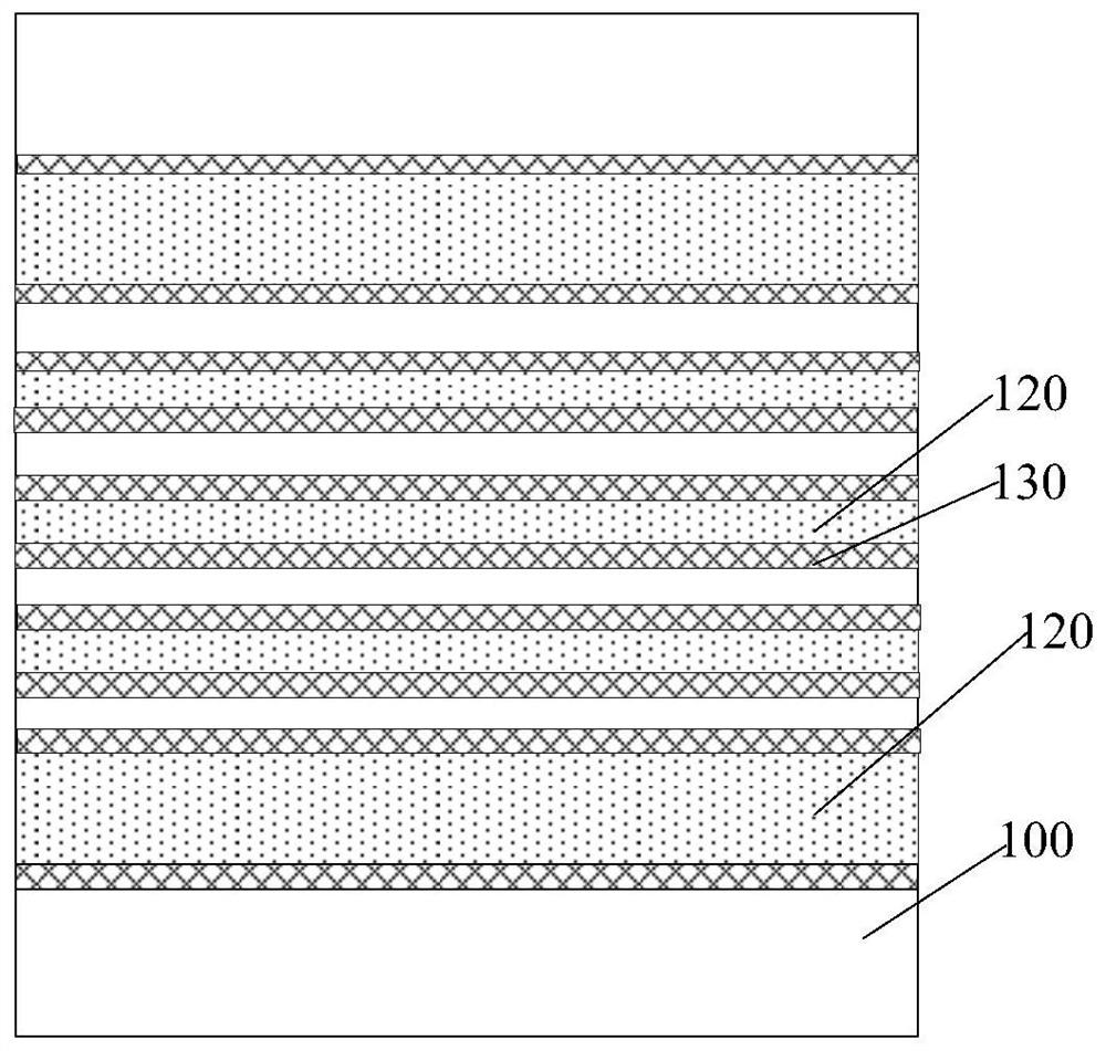
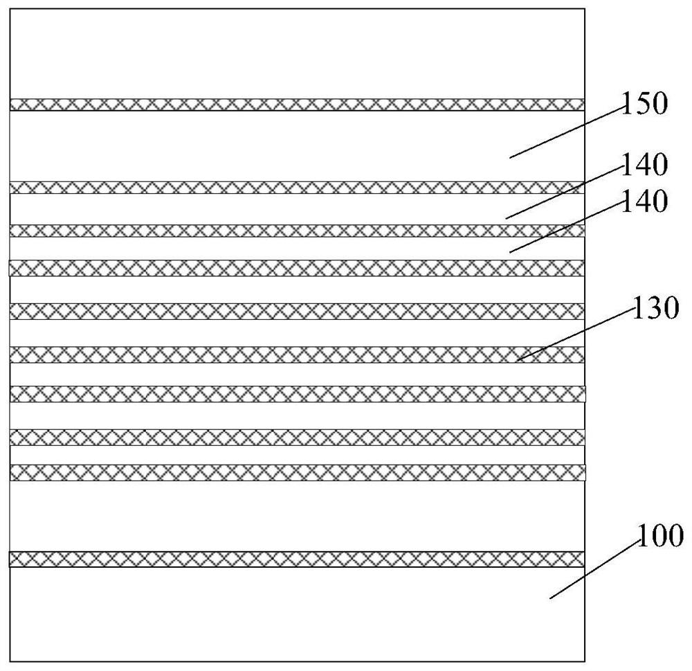
[0032] Figure 1 to Figure 3 It is a structural schematic diagram of the formation process of a semiconductor device.

[0033] refer to figure 1 , providing a dielectric layer 100 , the dielectric layer 100 includes a plurality of discrete first groove areas 101 and a plurality of second groove areas 102 , and the plurality of first groove areas 101 are located between adjacent second groove areas 102 .

[0034] refer to figure 2A sacrificial layer 120 is respectively formed on the first groove region 101 and the second groove region 102 of the dielectric layer 100 ; sidewalls 130 are formed on the sidewalls on both sides of the sacrificial layer 120 .

[0035] refer to image 3 , after forming the spacer 130, remove the sacrificial layer 120 (refer to figure 2 ); after removing the sacrificial layer 120, the dielectric layer 100 is etched with the sidewall 130 ...


PUM

PropertyMeasurementUnit
relative permittivityaaaaaaaaaa

Abstract

A semiconductor device and a method for forming the same, the method comprising: obtaining a plurality of discrete contact hole regions in a second groove region; obtaining a second groove modification region located in the second groove region according to the position of the contact hole region; The width of the correction area is smaller than the width of the second groove area; a sacrificial layer is respectively formed on the second groove correction area and the first groove area of ​​the dielectric layer; a first side wall and a second side wall are formed on the dielectric layer; on the second side A barrier layer is formed on the second groove area exposed by the wall, and the distance from the edge of the barrier layer to the edge of the sacrificial layer on the adjacent first groove area is equal to the minimum distance between the first side wall and the second side wall; sacrificial layer; then use the barrier layer, the first sidewall and the second sidewall as masks to etch the dielectric layer, form the first groove in the dielectric layer on both sides of the first sidewall, and form the first groove in the dielectric layer in the second groove correction area of ​​the dielectric layer A second groove is formed in the middle. The performance of the semiconductor device is improved.

Description

technical field [0001] The invention relates to the field of semiconductor manufacturing, in particular to a semiconductor device and a forming method thereof. Background technique [0002] With the continuous advancement of semiconductor integrated circuit process technology, when semiconductor devices are reduced to a deep submicron range, high-performance, high-density connections between semiconductor devices need to be realized through interconnect structures. It is easy to form parasitic resistance and parasitic capacitance in the interconnection structure, resulting in parasitic effect, which leads to the time delay of metal connection transmission. People are faced with how to overcome the RC caused by the rapid growth of connection length (R refers to resistance, C refers to capacitance) A problem with significantly increased latency. [0003] In order to overcome the parasitic effect in the interconnection, in the integrated process of the back-end process interco...

Claims


Application Information

Patent Timeline
Patent Type & Authority Patents(China)
IPC IPC(8): H01L21/768H01L23/528H01L23/535
CPCH01L21/76838H01L21/76877H01L23/528H01L23/535
Inventor 杨青
Owner SEMICON MFG INT (SHANGHAI) CORP
Why Eureka
Try Eureka