Silicon substrate cleaning method

A silicon substrate, water rinsing technology, used in electrical components, semiconductor/solid-state device manufacturing, circuits, etc., can solve problems such as poor, easy to corrode, destroying the cleaning effect of the oxide layer, etc., to achieve high uniformity, low cleaning cost, cleaning good effect

Active Publication Date: 2019-09-06
SHENZHEN XIWAN TECH CO LTD
View PDF5 Cites 0 Cited by
  • Summary
  • Abstract
  • Description
  • Claims
  • Application Information

AI Technical Summary

Problems solved by technology

[0003] The purpose of the present invention is to provide a silicon substrate cleaning method that can be used in the carbon nanotube industry, aiming to solve the problem that the existing cleaning technology is easy to corrode and damage the oxide layer on the surface of the silicon substrate and the cleaning effect is not good

Method used


Image

  • Silicon substrate cleaning method
  • Silicon substrate cleaning method

Examples


Embodiment 1

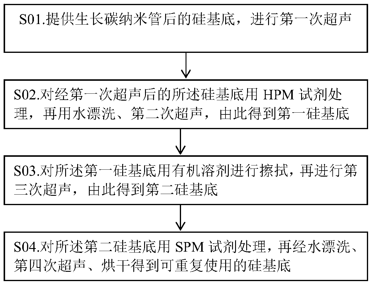
[0034] Provide 50 pieces of silicon substrates grown by carbon nanotubes, and use pure water to sonicate for 5 minutes at a frequency of 40 Hz; place the flower basket containing silicon chips in a quartz boat containing HPM reagents, the temperature of the reagents is 70 ° C, soak for 15 minutes, The HPM reagent is a volume ratio of DIW: hydrogen peroxide: hydrochloric acid = 6:1:1; rinse the silicon wafer with pure water for 5 minutes, and then use pure water to sonicate at a frequency of 40 Hz for 5 minutes to remove excess impurities; use a class 100 dust-free Dip the cloth with absolute ethanol, gently wipe the surface of the silicon wafer, remove the carbon nanotubes and amorphous carbon attached to the silicon wafer, and prevent them from being carried into the next process, and then use pure water at a frequency of 40 Hz for 5 minutes; Place the flower basket of silicon wafers in a quartz boat with SPM reagent at a temperature of 110°C and soak for 15 minutes. The SPM r...


PUM


Abstract

The invention provides a silicon substrate cleaning method, which comprises the following steps: providing a silicon substrate, and carrying out ultrasonic processing; processing the silicon substrateobtained after ultrasonic processing with an HPM reagent, and carrying out water rinsing and ultrasonic processing to obtain a first silicon substrate; wiping the first silicon substrate with absolute ethyl alcohol, and carrying out ultrasonic processing again to obtain a second silicon substrate; and processing the second silicon substrate with an SPM reagent, and carrying out water rinsing, ultrasonic processing and drying to obtain a reusable silicon substrate. After cleaning, silicon wafers are uniform and consistent in surface color, and have no spot and grey mark problems; and growth test of secondary carbon nanotubes shows that yield of the CNTs is lower than the yield of CNTs prepared through the new silicon wafers only by 4.5%, array height is lower than that of the new silicon wafers by 2.9%, and target requirements are basically met.

Description

technical field [0001] The invention relates to a silicon chip cleaning process, in particular to a cleaning method for a silicon substrate used for growing carbon nanotubes. Background technique [0002] In the prior art, a traditional industrial standard wet cleaning process (RCA cleaning method) is generally used to clean the silicon substrate. This method was proposed by Kem and Puotinen of Radio Corporation of America (RCA) in the 1960s. It mainly removes metals and organic substances on the surface of silicon wafers, and can also remove pollutants such as small particles. RCA is cleaned in the order of alkali-strong acid-weak acid. Generally, the first step is to add alkaline solution as SC-1, and the SC-1 solution includes H 2 o 2 and NH 4 OH, to remove organic contamination on the surface of the silicon wafer (organic matter will cover part of the surface of the silicon wafer, making it difficult to remove the oxide film and related contamination); the second step...

Claims


Application Information

Patent Timeline
IPC IPC(8): H01L21/02
CPCH01L21/02052
Inventor 邓飞
Owner SHENZHEN XIWAN TECH CO LTD
Why Eureka
Try Eureka