Self-alignment integrated package method of high-density three-dimensional lamination layer

An integrated packaging and self-alignment technology, applied in the manufacturing of electrical components, electrical solid-state devices, semiconductor/solid-state devices, etc., can solve the problems of poor thermal matching of circuit boards, high packaging costs, solder joint fatigue, etc., and reduce alignment Difficulty, small alignment difficulty, and the effect of reducing the failure rate

Pending Publication Date: 2019-09-06
10TH RES INST OF CETC
View PDF6 Cites 9 Cited by
  • Summary
  • Abstract
  • Description
  • Claims
  • Application Information

AI Technical Summary

Problems solved by technology

Disadvantages of PBGA (plastic BGA) packaging: sensitive to moisture, not suitable for packaging of devices with airtightness requirements and high reliability requirements
Disadvantages of CBGA (ceramic BGA) package: (1) Due to the different thermal expansion coefficients, the thermal matching with the epoxy resin printed circuit board is poor, and solder joint fatigue is the main failure mode
(2) The alignment of the solder balls at the edge of the package is difficult
(3) High packaging cost
Due to the high-density integration of multiple bare chips or packages, and the use of a variety of different functional materials in the package, the electromagnetic field distribution in the package is very complicated, which is likely to cause severe isolation, signal waveform distortion and other signal integrity and power integrity. problems, as well as EMI / EMC problems, which make the design of 3D packaging structure more complicated

Method used


Image

  • Self-alignment integrated package method of high-density three-dimensional lamination layer
  • Self-alignment integrated package method of high-density three-dimensional lamination layer
  • Self-alignment integrated package method of high-density three-dimensional lamination layer

Examples


Embodiment Construction

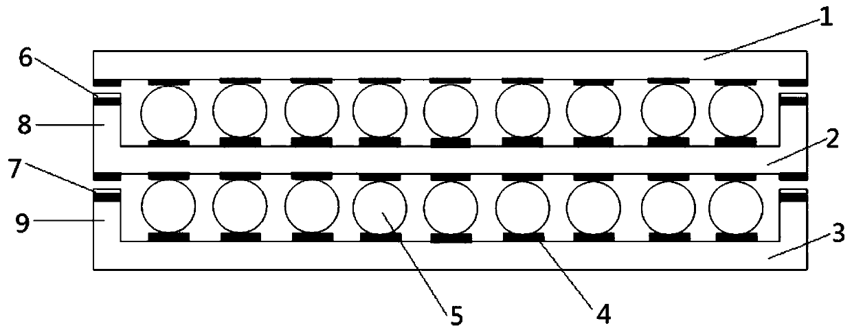
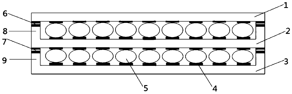
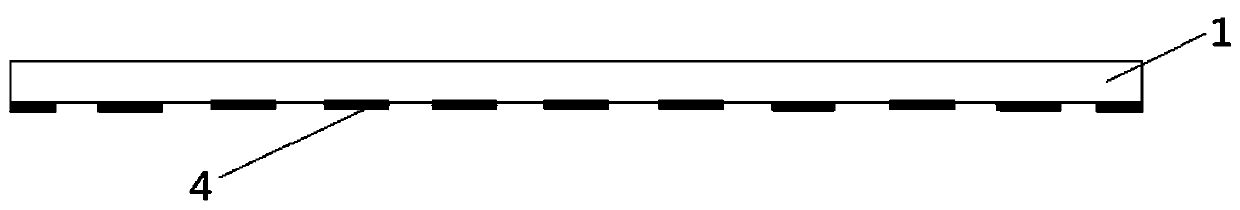
[0031] refer to Figure 1-Figure 5 . According to the present invention, the packaging structure is composed of three parts: a multilayer substrate, a boss on the periphery of the substrate, and micro BGA solder balls. The lower surface of the top substrate 1, the upper and lower surfaces of the middle substrate 2 and the upper surface of the bottom substrate 3 There are a large number of pads 4 for soldering micro BGA solder balls. The lower surface of the top substrate 1, the upper and lower surfaces of the intermediate substrate 2 and the upper surface of the bottom substrate 3 are evenly distributed with a large number of micro BGA ball pads 4 for soldering micro BGA solder balls, and the micro BGA solder balls are attached to the intermediate layer The upper surface of the substrate 2 and the bottom substrate 3, the micro BGA ball pads 4 on the upper surface of the intermediate substrate 2 correspond to the micro BGA ball pads 4 on the lower surface of the top substrate ...


PUM


Abstract

The invention discloses a self-alignment integrated package method of a high-density three-dimensional lamination layer, and aims to provides an integrated package method which employs a BGA welding ball as an interlayer mechanical support for multi-layer substrate self-alignment three-dimensional stack and also can be a signal interconnection passage among high-density layers. The self-alignmentintegrated package method is implemented according to the technical scheme that bonding pads are arranged on a lower surface of a top-layer substrate, an upper surface and a lower surface of an intermediate-layer substrate and an upper surface of a bottom-layer substrate and are used for welding micro BGA welding balls, the micro BGA welding balls are attached onto the upper surface of the intermediate-layer substrate and the upper surface of the bottom-layer substrate, the micro BGA welding balls on the upper surface of the intermediate-layer substrate are corresponding to the lower surface of the top-layer substrate, the micro BGA welding balls on the upper surface of the bottom-layer substrate are corresponding to the lower surface of the intermediate-layer substrate, vertical and interconnection rectangular array micro BGA ball welding is formed, a hollow square boss cavity box body is arranged at the peripheries outside an upper cavity surface of the intermediate-layer substrate 2and an upper cavity surface of the bottom-layer substrate 3, the cavity box body is stacked and placed in a backflow welding furnace by a tool, and self-alignment lamination layer welding is performed to form a package body.

Description

technical field [0001] The invention relates to microsystem integrated packaging technology in the field of system-level packaging. The invention is a high-density self-aligned three-dimensional integrated packaging method based on micro ball grid array packaging. This technology is especially suitable for multi-layer packaging that requires interlayer signal interconnection and transmission. Substrate stacking and packaging. Background technique [0002] The packaging technology of electronic devices is a key link restricting the development of integrated circuits. Electronic packaging is to provide protection for various functional chips, components and carrier substrates and ensure the input and output of signals and power. At the same time, the heat generated during the operation of the device is transferred to the external environment to ensure the stable and normal operation of the device. In recent years, with the rapid development of system-in-package technology and...

Claims


Application Information

Patent Timeline
Patent Type & Authority Applications(China)
IPC IPC(8): H01L21/56H01L21/67H01L23/31H01L23/498H01L23/538H01L21/60
CPCH01L21/561H01L21/67121H01L23/3121H01L23/49822H01L23/5383H01L24/27H01L24/30H01L2224/273H01L2224/27H01L2224/80815
Inventor 邱钊朱勇张先荣
Owner 10TH RES INST OF CETC
Why Eureka
Try Eureka