
Double-sided in-situ measurement system and method for charge distribution in thin dielectric film

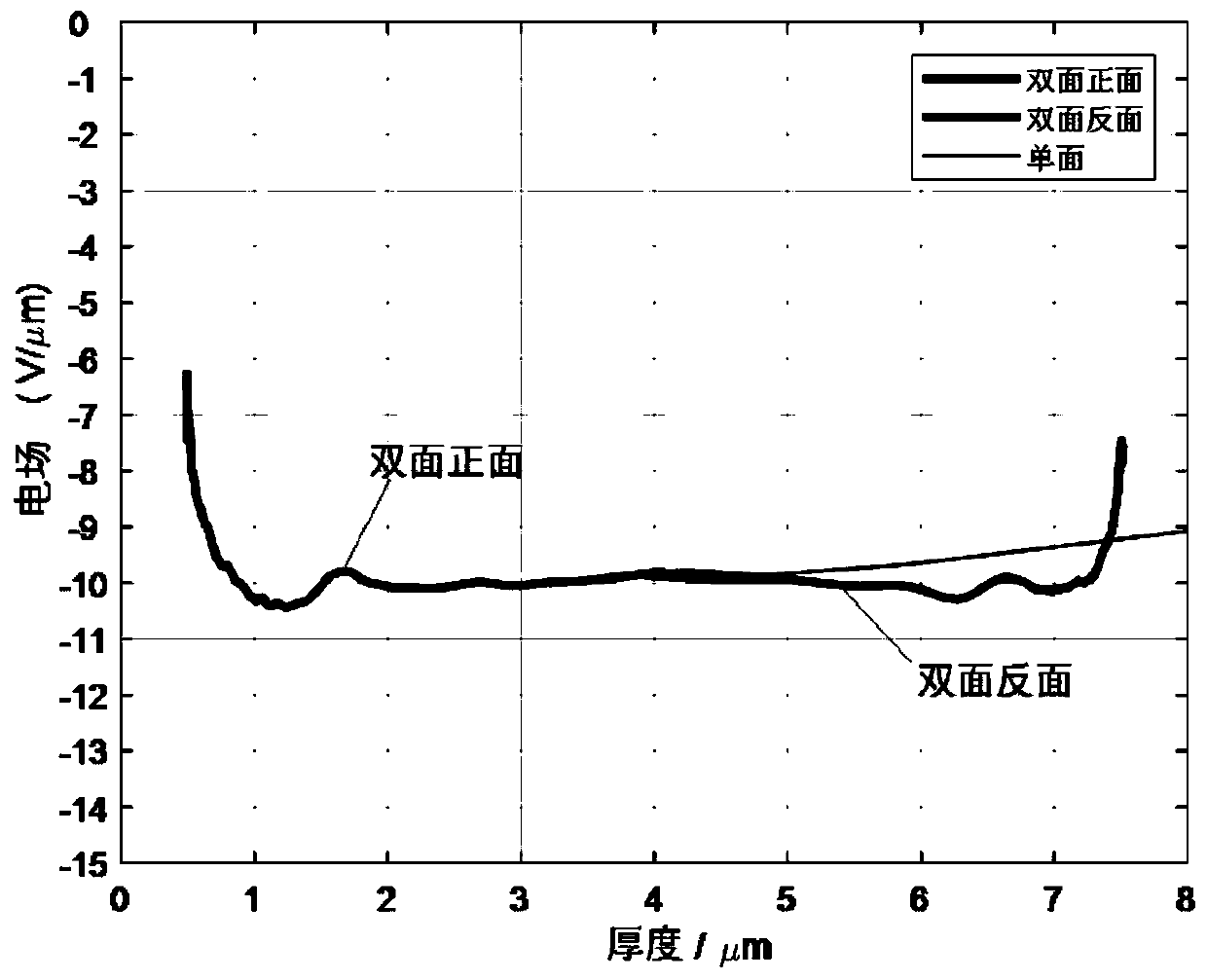
A technology of charge distribution and in-situ measurement, which is applied in the direction of electrostatic field measurement, measuring device, and electric variable measurement, can solve the problem of lower resolution, reduce resolution drop, achieve accurate measurement results, and improve spatial resolution Effect

Pending Publication Date: 2019-09-17
TONGJI UNIV
View PDF11 Cites 6 Cited by
  • Summary
  • Abstract
  • Description
  • Claims
  • Application Information

AI Technical Summary

Problems solved by technology

[0006] The object of the present invention is to provide a double-sided in-situ measurement system and method for charge distribution in a dielectric thin film in order to overcome the defect of the thermal pulse method in the prior art that the resolution decreases along the direction of heat conduction.

Method used


Image

  • Double-sided in-situ measurement system and method for charge distribution in thin dielectric film
  • Double-sided in-situ measurement system and method for charge distribution in thin dielectric film

Examples


Embodiment

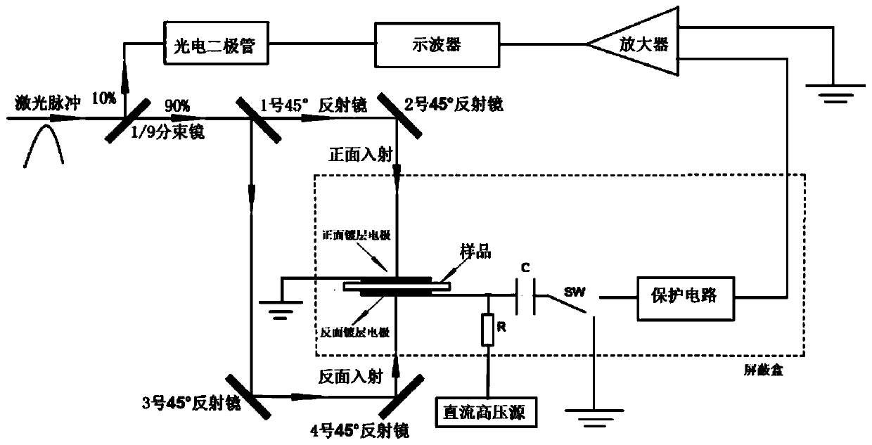
[0030] Such as figure 1 As shown, this application proposes a double-sided in-situ measurement system for charge distribution in a dielectric film, including a sample to be tested, a pulsed laser, a photoelectric trigger circuit, a double-sided measurement optical path, a pressurizing circuit, and a measuring circuit.

[0031] The sample to be tested is a dielectric film with metallized electrodes vapor-deposited on both sides. The double-sided electrode of the dielectric film can be metallized by magnetron sputtering or thermal evaporation to obtain a front-side coating electrode and a back-side coating electrode. The double-sided plated electrodes can be metals with good conductivity such as aluminum, gold, silver, etc., and the thickness should be as thin as possible, subject to opacity. The selection of the electrode diameter is based on the principle that the capacitance of the dielectric film is relatively small without causing distortion of the measurement signal. In ...


PUM


Abstract

The invention relates to a double-sided in-situ measurement system and method for charge distribution in a thin dielectric film, and the system comprises a sample to be tested, a pulse laser, a photoelectric trigger circuit, a double-sided measuring optical path, a pressurizing circuit and a measuring circuit, wherein the laser generated by the pulse laser is divided into two paths, which respectively enter the photoelectric trigger circuit and the double-sided measuring optical path; the double-sided measuring optical path respectively injects the laser into a front plating electrode and a reverse plating electrode in two directions; the pressurizing circuit comprises a DC high voltage source that is applied to the reverse plating electrode of the thin dielectric film through a current limiting resistor, the reverse plating electrode is also connected to the movable end of a single-pole double-throw switch through a coupling capacitor, two fixed ends are respectively connected to the ground and a protection circuit, the protection circuit is connected to the measuring circuit, and the front plating electrode is grounded. Compared with the prior art, the invention greatly reduces the problem of the reduced resolution of the thermal pulse method in the direction of incidence of light, and improves the spatial resolution of the measurement as a whole.

Description

technical field [0001] The invention relates to a measurement technology of charge distribution in a dielectric thin film, in particular to a double-sided in-situ measurement system and method for charge distribution in a dielectric thin film based on a thermal pulse method. Background technique [0002] Dielectric films have many advantages, such as good insulation performance, strong resistance to mechanical stress, high pressure and temperature resistance, light weight, etc., so they are widely used as insulating dielectric layers for electrical equipment such as capacitors. Under the external DC high electric field, the phenomenon of space charge accumulation inside the dielectric film cannot be ignored. The accumulated charge will distort the original uniform electric field inside the dielectric, affecting the safety and reliability of electrical equipment such as capacitors. [0003] The heat pulse method is a method for measuring the electric field and space charge de...

Claims


Application Information

Patent Timeline
IPC IPC(8): G01R29/14G01R29/24
CPCG01R29/14G01R29/24
Inventor 郑飞虎谢姣张冶文
Owner TONGJI UNIV
Learn More