A semiconductor structure, image sensor, chip and method for forming the same

An image sensor and semiconductor technology, applied in the direction of semiconductor devices, semiconductor/solid-state device manufacturing, semiconductor/solid-state device components, etc., can solve the problems of easy damage or failure of chips, reduced yield rate of image sensors, and increased manufacturing costs of image sensors, etc. , to achieve the effect of a wide range of application environments and flexible cutting methods

Active Publication Date: 2021-07-30
ICLEAGUE TECH CO LTD
View PDF6 Cites 0 Cited by
  • Summary
  • Abstract
  • Description
  • Claims
  • Application Information

AI Technical Summary

Problems solved by technology

[0004] However, the chip of the image sensor is easily damaged or fails during the manufacturing process, which leads to a decrease in the overall yield of the image sensor and increases the manufacturing cost of the image sensor.

Method used


Image

  • A semiconductor structure, image sensor, chip and method for forming the same
  • A semiconductor structure, image sensor, chip and method for forming the same
  • A semiconductor structure, image sensor, chip and method for forming the same

Examples


Embodiment Construction

[0047] As described in the background art, it is necessary to improve the yield rate of image sensors and reduce the manufacturing cost of image sensor chips.

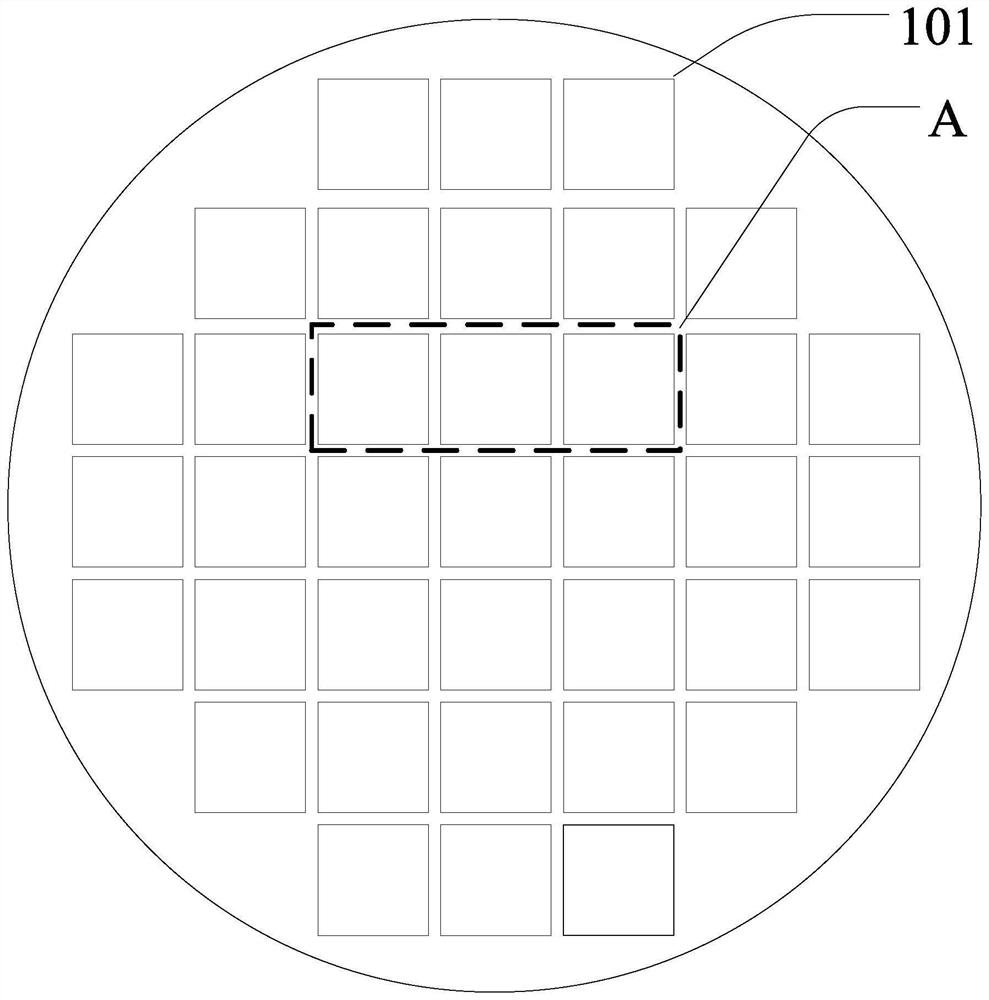
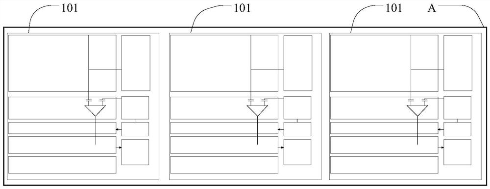
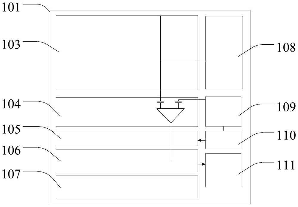
[0048] figure 1 It is a schematic diagram of the top view structure of a wafer with an image sensor chip, figure 2 yesfigure 1 The local enlarged schematic diagram of region A in the wafer, image 3 yes figure 1 Schematic diagram of the structure of the chip area in area A of the wafer.

[0049] Please refer to Figure 1 to Figure 3 , the wafer with the image sensor chip includes: a wafer 100, the wafer 100 includes a number of independent chip areas 101 separated from each other; the independent chip area 101 includes: an independent chip area pixel array unit 103, an independent chip area Comparison loop unit 104, independent chip area timing and control unit 105, independent chip area memory unit 106, independent chip area row selection unit and column selection unit 107, independent chip area data transmission...


PUM


Abstract

A semiconductor structure, a method for forming an image sensor chip, an image sensor chip, and an image sensor, the structure comprising: a substrate, the substrate including a plurality of chip regions separated from each other; each of the chip regions It includes more than 4 mutually separated device areas, each of which includes a pixel array unit, and at least 2 pixel array units are adjacent to each other in each chip area. The semiconductor structure improves the yield of the image sensor.

Description

technical field [0001] The invention relates to the technical field of semiconductors, in particular to a semiconductor structure, a method for forming an image sensor chip, an image sensor chip and an image sensor. Background technique [0002] In the field of semiconductor technology, an image sensor is a functional device that converts an optical image into an electrical signal. Image sensors can be roughly classified into charge coupled devices (charge coupled device, CCD) and complementary metal oxide semiconductor image sensors (CMOS Image Sensor, CIS). [0003] At present, CCD is the main practical solid-state image sensor device, which has the advantages of low reading noise, large dynamic range and high response sensitivity. CMOS image sensors are widely used in digital cameras, camera phones, digital video cameras, medical imaging devices (such as gastroscopes), automotive In the field of camera equipment and so on. [0004] However, the chip of the image sensor...

Claims


Application Information

Patent Timeline
Patent Type & Authority Patents(China)
IPC IPC(8): H01L23/544H01L21/66H01L21/78
CPCH01L21/78H01L22/22H01L22/24H01L22/34
Inventor 姚公达
Owner ICLEAGUE TECH CO LTD
Why Eureka
Try Eureka