
PCB mounting process and mounting glue applied to mounting process

A technology of PCB board and patch glue, which is applied in the direction of assembling printed circuit of electrical components, electrical components, printed circuit manufacturing, etc. It can solve the problem of indetermination of curing temperature of epoxy resin, weakening of transition metal ion activity, and inability to guarantee the degree of curing And other problems, to speed up the light curing speed, reduce the time, reduce the effect of irreversible damage

Active Publication Date: 2019-09-17
深圳市英创立电子有限公司
View PDF4 Cites 1 Cited by
  • Summary
  • Abstract
  • Description
  • Claims
  • Application Information

AI Technical Summary

Problems solved by technology

When the imidazole curing agent is mixed with the transition metal inorganic salt additive, the complex formed by the transition metal ion and imidazole will weaken the activity of the transition metal ion, thereby improving the storage performance of the adhesive; After the PCB board of the adhesive enters the reflow oven, the complex will affect the active temperature of the curing agent, and the temperature at which the complex begins to react cannot be determined, that is, the temperature at which the epoxy resin begins to cure cannot be determined, so that it is impossible to ensure that the adhesive enters the reflow The degree of curing before the weld zone

Method used


Image

  • PCB mounting process and mounting glue applied to mounting process
  • PCB mounting process and mounting glue applied to mounting process
  • PCB mounting process and mounting glue applied to mounting process

Examples


Embodiment 1-12

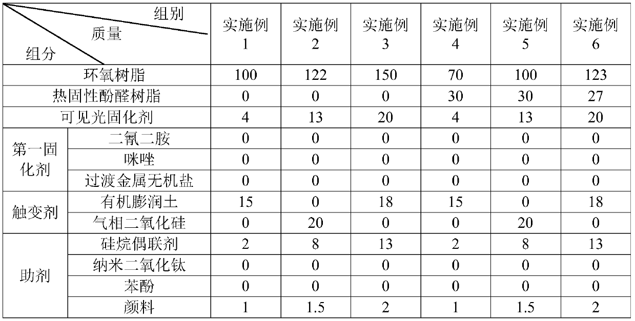
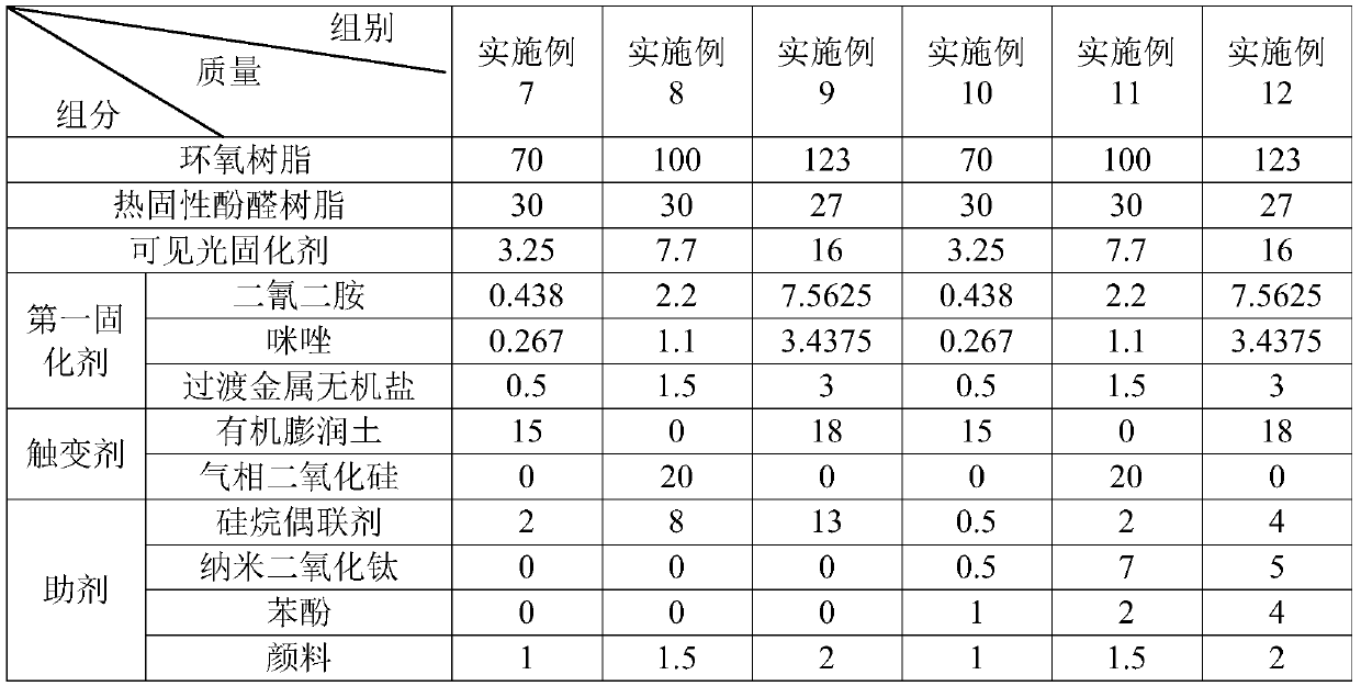
[0048] Example 1-12: A patch adhesive. The components included in Examples 1-6 and the corresponding masses are shown in Table 1, and the components and corresponding masses included in Examples 7-12 are shown in Table 2. And made by the following steps:

[0049] Step 1: Mix the epoxy resin, thermosetting phenolic resin, thixotropic agent, and auxiliary agent, stir at 300r / min for 2h under the environment of 30±1℃ and the vacuum degree of 0.05MPa to obtain the mixture A;

[0050] Step 2: Add the visible light curing agent and the first curing agent to the mixture A, and stir at 50r / min for 1h in a closed environment.

[0051] Table 1 Example 1-6 components and corresponding mass (kg)

[0052]

[0053] Table 2 Example 7-12 components and corresponding mass (kg)

[0054]

[0055] In the above embodiment,

[0056] The visible light curing agent is obtained by mixing the diaryliodonium salt and the dye at a weight ratio of 2:1.

[0057] The transition metal inorganic salt in Examples 7-9 is ...

Embodiment 13

[0059] Embodiment 13: A PCB board placement process, including the following steps:

[0060] S1: Print solder paste on the A side of the PCB board;

[0061] S2: Place the adhesive on the A side of the PCB board, mount the components on the A side, and enter the reflow oven with the A side up for reflow soldering;

[0062] S3: Print solder paste on the B side of the PCB, mount the components on the B side, and enter the reflow oven with the B side up for reflow soldering;

[0063] Illumination equipment is installed on both sides of the inner cavity of the reflow oven, the illumination equipment is located on both sides of the conveyor belt, and the illumination equipment is installed in front of the reflow soldering area;

[0064] The residence time of PCB A side in the heating zone is 2min in total;

[0065] Among them, the reflow furnace includes a heating zone, a reflow soldering zone and a cooling zone in sequence. The starting temperature of the heating zone is 30±1℃ and the final t...

Embodiment 14

[0067] Embodiment 14: A PCB board placement process, which is different from Embodiment 13 in that the residence time of the PCB board A surface in the heating zone is 2.3 min in total.


PUM


Abstract

The invention discloses a PCB mounting process and a mounting glue applied to the mounting process, belonging to the field of PCBs. The problem that an additive affects the curing degree of epoxy resin in the prior art is solved. The mounting process includes the following steps of (S1) printing a solder paste on an A side of a PCB, (S2) dispensing the mounting glue to the A side of the PCB, mounting components of the A side, and allowing the PCB to enter a reflow furnace with A side up for reflow soldering, and (S3) printing a solder paste on a B side of the PCB, mounting components of the B side, and allowing the PCB to enter the reflow furnace with B side up for reflow soldering, wherein illumination equipment is set in the reflow furnace and is arranged in front of a reflow soldering zone in the reflow furnace and is at two sides of a conveyor belt, and the residence time of the A side of the PCB in a heating zone is 2 to 4 minutes. The mounting glue can achieve a sufficient degree of curing before the components in the obtained PCB of the present invention enter the reflow soldering zone.

Description

Technical field [0001] The invention relates to the field of PCB boards, in particular to a PCB board mounting process and a patch glue used in the mounting process. Background technique [0002] PCB board, also known as circuit board, printed circuit board, replaces the wiring method by printing; PCB board miniaturizes, centralizes and simplifies the circuit of complex wiring and electronic parts. The PCB board includes a single-sided board with parts concentrated on one side, a double-sided board with parts distributed on both sides, and a multilayer board that can increase the wiring area. [0003] When making a double-sided PCB board, because the A and B sides of the PCB board need to be printed and sent to the reflow oven in sequence; the PCB board is placed on the conveyor belt, and the PCB board goes through the heating zone and reflow soldering in the reflow oven. Zone and cooling zone. If the solder paste printing and reflow soldering are performed on the A side first, th...

Claims


Application Information

Patent Timeline
Patent Type & Authority Applications(China)
IPC IPC(8): H05K3/34
CPCH05K3/341H05K3/3494
Inventor 王启胜赵林森刘德荣宋日新夏明明
Owner 深圳市英创立电子有限公司
Learn More