Two-dimensional transition metal chalcogenide crystal, and preparation method and application thereof

A transition metal chalcogenide, transition metal technology, applied in the fields of electronics and optoelectronics, can solve the problems of difficult control of nucleation and growth, complex process, poor product uniformity, etc.

Active Publication Date: 2019-09-20
NORTHWESTERN POLYTECHNICAL UNIV
View PDF6 Cites 14 Cited by
  • Summary
  • Abstract
  • Description
  • Claims
  • Application Information

AI Technical Summary

Problems solved by technology

[0003] The preparation of materials determines the future. The controllable preparation of large-area, uniform-thickness, high-quality two-dimensional transition metal chalcogenide materials is the basis for its research and application, but there are still challenges such as nucleation and growth that are difficult to control.
[0004] CN106757361A disc

Method used


Image

  • Two-dimensional transition metal chalcogenide crystal, and preparation method and application thereof
  • Two-dimensional transition metal chalcogenide crystal, and preparation method and application thereof
  • Two-dimensional transition metal chalcogenide crystal, and preparation method and application thereof

Examples


Embodiment 1

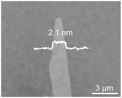
[0068] Preparation of two-dimensional transition metal chalcogenide crystals

[0069] (1) In a tube furnace with a single temperature zone, a quartz crucible filled with 60 mg of Te elemental powder with a particle size of 100 mesh is placed on the upstream of 15 cm from the center, and a layer of Te elemental powder with an effective aperture of The particle size of 3mg of molecular sieve is 300 mesh MoO 3 The powdered cubic ceramic crucible will have a layer of 280nm SiO on the surface 2 The silicon substrate is placed on the top of the cubic ceramic crucible, and retains a slit accounting for 15% of the cubic ceramic crucible mouth area for the entry and exit of airflow;

[0070] (2) Into the tube furnace with a flow rate of 20 sccm and hydrogen of 10 sccm, and the tube furnace is heated to 800 ° C at a rate of 30 ° C / min, so that the precursor Te elemental powder is placed The temperature at the place is 450°C, keep the temperature for 10min, and carry out chemical va...

Embodiment 2

[0074] The difference from Example 1 is that the temperature of the tube furnace was raised to 750°C.

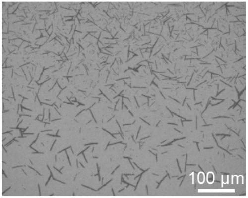
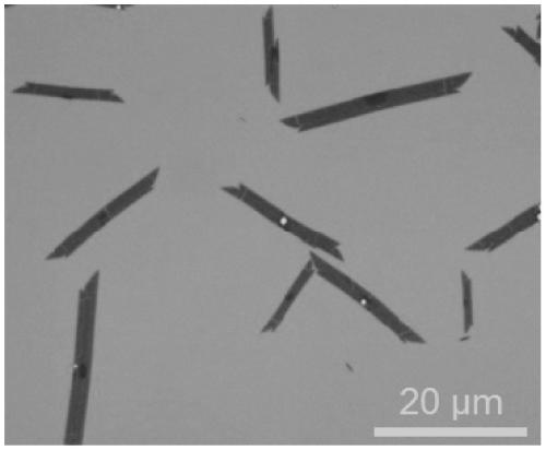
[0075] Figure 4 It is the 1T'MoTe obtained in Example 2 2 The optical photo of the crystal, it can be seen from the figure that the 1T'MoTe 2 The crystals are polycrystalline with a maximum dimension of about 18 μm.

Embodiment 3

[0077] The difference from Example 1 is that the temperature of the tube furnace was raised to 650°C.


PUM

PropertyMeasurementUnit
Particle sizeaaaaaaaaaa
Thicknessaaaaaaaaaa
Thicknessaaaaaaaaaa

Abstract

The invention relates to a two-dimensional transition metal chalcogenide crystal, and a preparation method and application thereof. The preparation method includes the following steps: (1) sequentially putting a chalcogen source and a transition metal oxide source along an airflow direction in a heating device, wherein the transition metal oxide source is coated with a molecular sieve, and a growth substrate is put on the upper side of the transition metal oxide source; (2) injecting a protective gas into the heating device, increasing the temperature until the temperature of the transition metal oxide source reaches a chemical vapor deposition temperature and the temperature of the chalcogen source reaches an elemental volatilization temperature, and performing chemical vapor deposition to obtain the two-dimensional transition metal chalcogenide crystal. The large-area uniform monolayer or multilayer two-dimensional transition metal chalcogenide crystal can be obtained by the preparation method and can be applied to polarized photoelectric detection or topological field effect transistors.

Description

technical field [0001] The invention relates to the technical fields of electronics and optoelectronics, in particular to a two-dimensional transition metal chalcogenide crystal and its preparation method and application. Background technique [0002] Two-dimensional transition metal dichalcogenides (TMDs) materials have a layered structure similar to graphene, covering a variety of materials with different properties, such as metallic 1T'MoTe 2 , WTe 2 etc., semiconducting MoS 2 、WSe 2 etc. and the Bi of the insulator 2 Se 3 Wait. Among them, most semiconducting two-dimensional TMDs materials have excellent properties such as layer number-dependent bandgap structure and high carrier mobility, which effectively make up for the shortcomings of graphene's zero bandgap, and are expected to be used in electronic and optoelectronic devices. get applied. [0003] The preparation of materials determines the future. The controllable preparation of large-area, uniform-thicknes...

Claims


Application Information

Patent Timeline
IPC IPC(8): C30B25/18C30B25/10C30B28/14C30B29/46
CPCC30B25/10C30B25/18C30B28/14C30B29/46
Inventor 冯晴亮朱美洁李萌郑建邦
Owner NORTHWESTERN POLYTECHNICAL UNIV
Why Eureka
Try Eureka