Oscillation circuit
A technique of oscillating circuits and circuits, applied in power oscillators, electrical components, adjusting electrical variables, etc., can solve the problems of circuit scale enlargement and oscillation frequency change, etc., and achieve the effect of small circuit scale and small influence of temperature
- Summary
- Abstract
- Description
- Claims
- Application Information
AI Technical Summary
Problems solved by technology
Method used
Image

Examples
no. 1 approach
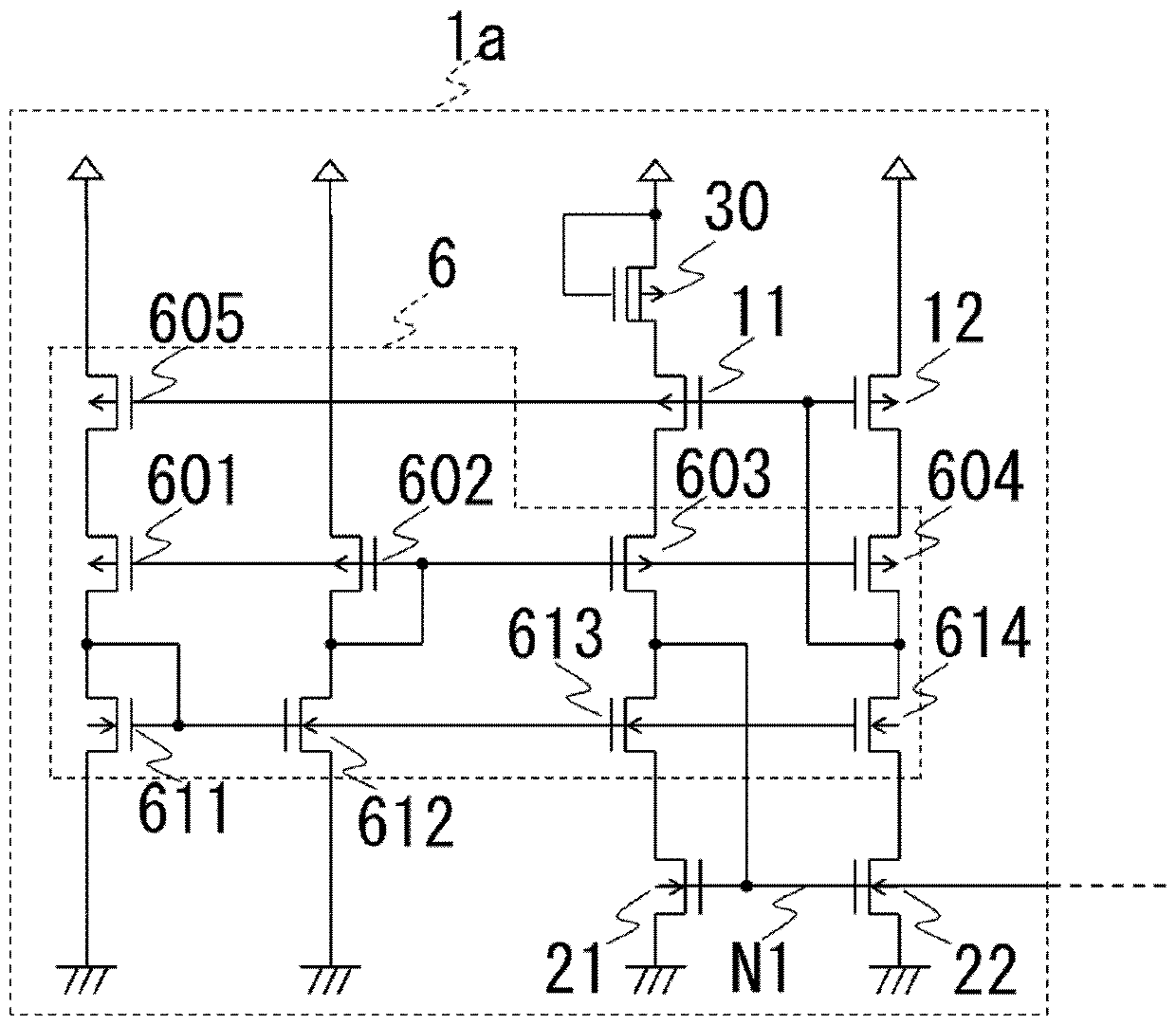
[0026] figure 1 It is a diagram showing an oscillation circuit 100 according to the first embodiment, and is composed of a constant current circuit 1 , a charging and discharging circuit 2 , and a control circuit 3 .
[0027] The constant current circuit 1 includes a depletion-type PMOS transistor 30 serving as a current source, enhancement-type PMOS transistors 11 and 12 serving as a current mirror circuit, and an enhancement-type NMOS transistor 21 serving as a current mirror circuit. , 22 forms. In the depletion-type PMOS transistor 30 , the source and the gate are connected to the first power supply VDD, and the drain is connected to the source of the PMOS transistor 11 . In the PMOS transistor 11 , the gate is connected to the gate of the PMOS transistor 12 , and the drain is connected to the drain and gate of the NMOS transistor 21 . The drain of the PMOS transistor 11 is referred to as a node N1. In the PMOS transistor 12 , the source is connected to the first power...
no. 2 approach
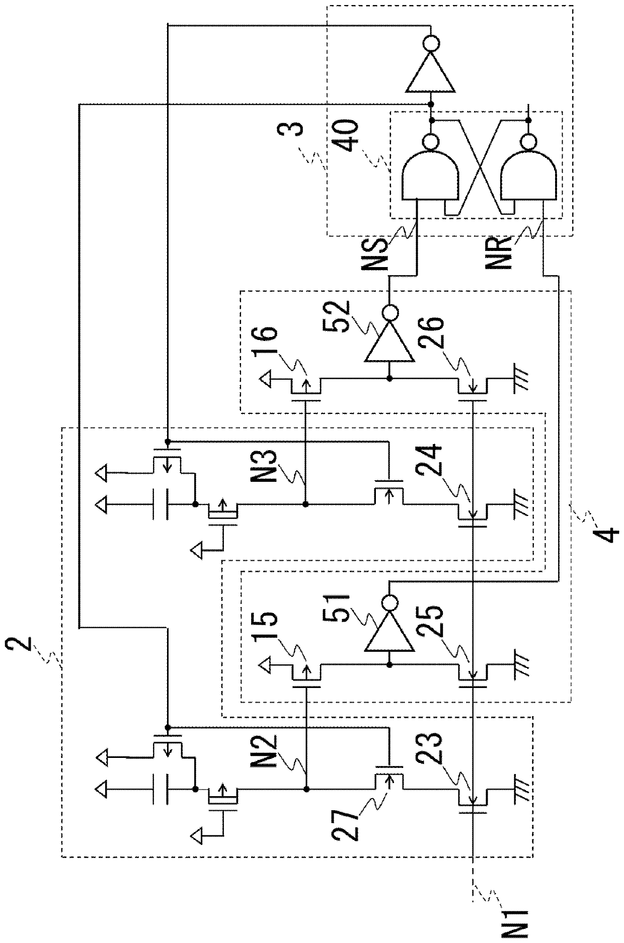
[0066] image 3 It is a diagram showing the charging and discharging circuit 2, the control circuit 3, and the waveform shaping circuit 4 of the oscillation circuit of the second embodiment. The second embodiment differs from the oscillation circuit 100 of the first embodiment in that the waveform shaping circuit 4 is provided, and is the same as the first embodiment in other respects. Description of the same parts as those of the first embodiment will be omitted.
[0067] The waveform shaping circuit 4 is composed of enhancement type PMOS transistors 15 , 16 , enhancement type NMOS transistors 25 , 26 , and inverters 51 , 52 .
[0068] In the PMOS transistor 15 , the source is connected to the first power supply VDD, the gate is connected to the node N2 , and the drain is connected to the NMOS transistor 25 and the input of the inverter 51 . In the NMOS transistor 25, the gate is connected to the node N1 of the constant current circuit, and the source is connected to the se...
no. 3 approach
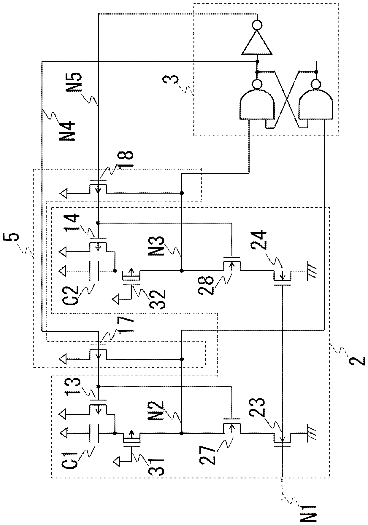
[0072] Figure 4 It is a diagram showing the charging and discharging circuit 2 , the control circuit 3 , and the voltage boost circuit 5 of the oscillation circuit of the third embodiment. The third embodiment differs from the oscillation circuit 100 of the first embodiment in that the voltage boosting circuit 5 is provided, and is the same as the first embodiment in other respects. Description of the same parts as those of the first embodiment will be omitted.
[0073] The voltage boosting circuit 5 is composed of enhancement type PMOS transistors 17 and 18 .
[0074] In the PMOS transistor 17, the source is connected to the first power supply VDD, the gate is connected to the node N4, and the drain is connected to the node N2. In the PMOS transistor 18, the source is connected to the first power supply VDD, the gate is connected to the node N5, and the drain is connected to the node N3.
[0075] The operation of this embodiment will be described. After explaining the oper...
PUM
 Abstract
Description
Claims
Application Information
 - Generate Ideas
- Intellectual Property
- Life Sciences
- Materials
- Tech Scout
- Unparalleled Data Quality
- Higher Quality Content
- 60% Fewer Hallucinations
Browse by: Latest US Patents, China's latest patents, Technical Efficacy Thesaurus, Application Domain, Technology Topic, Popular Technical Reports.
© 2025 PatSnap. All rights reserved.Legal|Privacy policy|Modern Slavery Act Transparency Statement|Sitemap|About US| Contact US: help@patsnap.com