

A single-carrier photodetector
A photodetector and single-carrier technology, applied in the field of photodetectors, can solve problems such as poor lattice quality and low frequency response bandwidth, and achieve the effects of low cost, high response speed, and stable device performance
- Summary
- Abstract
- Description
- Claims
- Application Information
AI Technical Summary
Problems solved by technology
Method used
Image

Examples
Embodiment
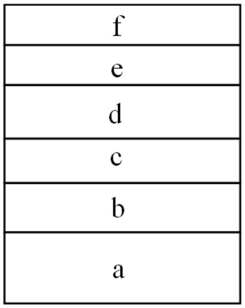
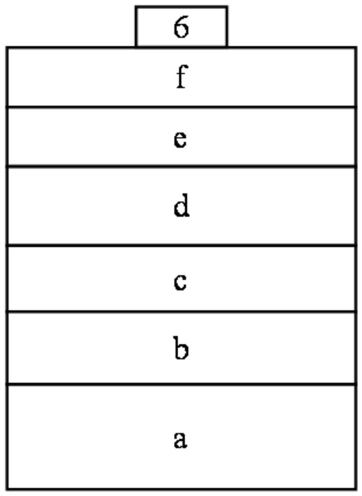
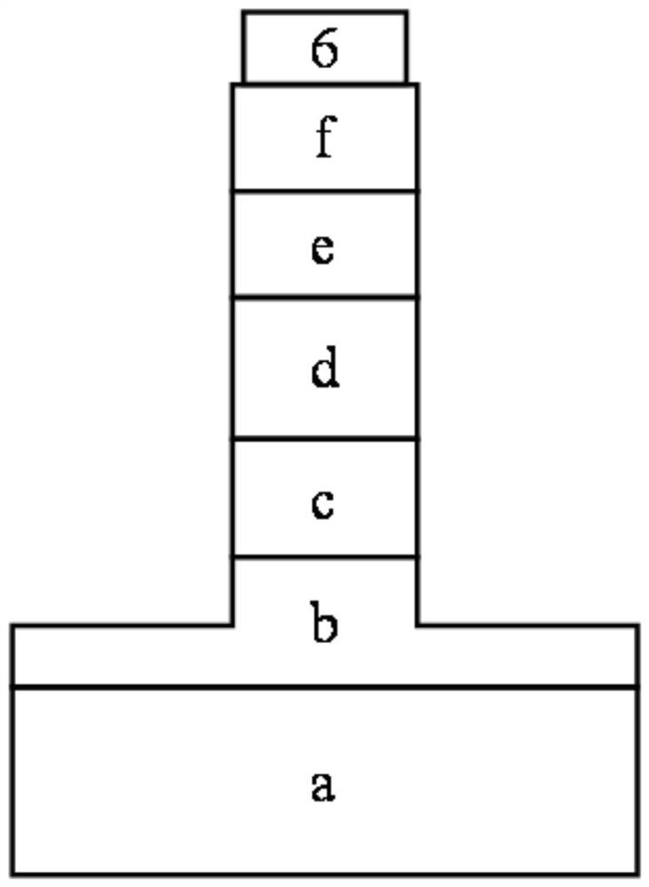
[0032] A method for preparing a single-carrier photodetector in a 2 μm band, comprising the following steps:
[0033] Step 1: Using molecular beam epitaxy to sequentially grow a cathode contact layer b, a collector layer c, an InGaAs / GaAsSb multi-quantum well absorption layer d, an electron blocking layer e, and an anode contact layer f on an InP substrate a, such as figure 1 Shown; The parameters of each growth layer are shown in Table 1:
[0034] Table 1
[0035]
[0036] It can be seen from Table 1 that the thickness of the cathode contact layer b is 900nm, and the doping concentration of one layer is 1×10 19 cm -3 The doping concentration of the N-type InP layer and one layer is 1×10 18 cm -3 The composition of the N-type InP layer, where the latter is used to reduce the diffusion of impurity ions to the InP collector layer;
[0037] The thickness of the collector layer c is 400nm, and the doping concentration is 1×10 16 cm -3 the following;
[0038]The structu...
PUM
| Property | Measurement | Unit |
|---|---|---|
| thickness | aaaaa | aaaaa |
| thickness | aaaaa | aaaaa |
| thickness | aaaaa | aaaaa |
Abstract
Description
Claims
Application Information