
Carbonized silicon single crystal growing device and method for producing carbonized silicon single crystal

A silicon carbide single crystal and growth device technology, which is applied in the direction of single crystal growth, single crystal growth, crystal growth, etc., can solve the problems of crystal quality decline, achieve the effect of improving quality, increasing crystal growth length, and improving growth efficiency

Active Publication Date: 2019-10-15
浙江富芯微电子科技有限公司
View PDF4 Cites 2 Cited by
  • Summary
  • Abstract
  • Description
  • Claims
  • Application Information

AI Technical Summary

Problems solved by technology

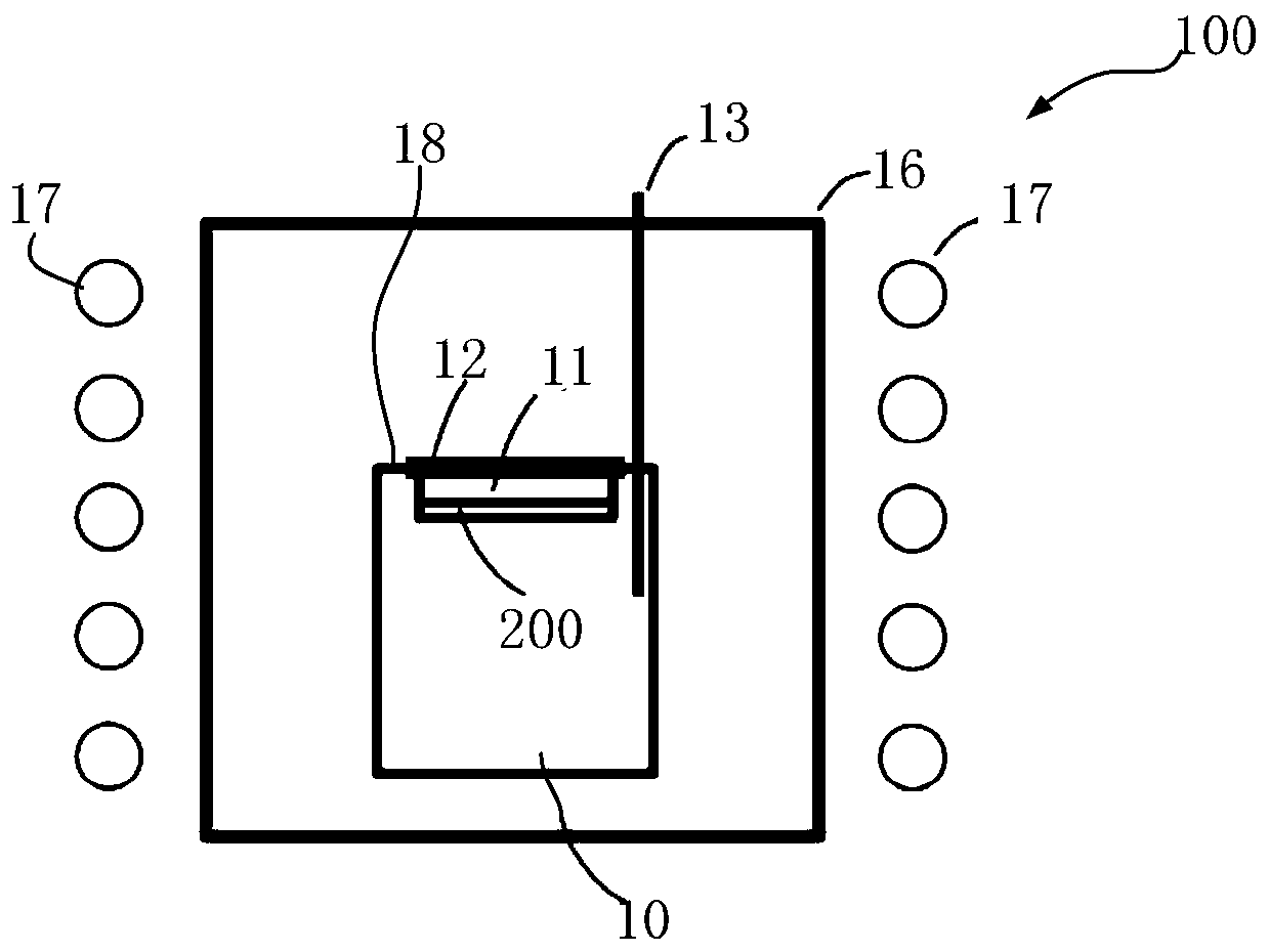
For this reason, the present invention proposes a silicon carbide single crystal growth device and a method for manufacturing a silicon carbide single crystal, which solves the problem of the crystal quality decline caused by the change of silicon carbide from silicon-rich to carbon-rich, increases the crystal growth length, and improves the crystal growth rate. benefit, so as to obtain high-quality silicon carbide single crystal

Method used

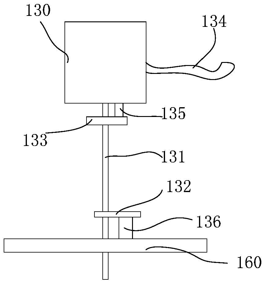

Image

  • Carbonized silicon single crystal growing device and method for producing carbonized silicon single crystal
  • Carbonized silicon single crystal growing device and method for producing carbonized silicon single crystal
  • Carbonized silicon single crystal growing device and method for producing carbonized silicon single crystal

Examples


Embodiment Construction

[0039] Exemplary embodiments of the present disclosure will be described in more detail below with reference to the accompanying drawings. Although exemplary embodiments of the present disclosure are shown in the drawings, it should be understood that the present disclosure may be embodied in various forms and should not be limited by the embodiments set forth herein. Rather, these embodiments are provided for more thorough understanding of the present disclosure and to fully convey the scope of the present disclosure to those skilled in the art.

[0040] It should be understood that the terminology used herein is for the purpose of describing particular example embodiments only and is not intended to be limiting. As used herein, the singular forms "a", "an" and "the" may also be meant to include the plural forms unless the context clearly dictates otherwise. The terms "comprising", "comprising" and "having" are inclusive and thus indicate the presence of stated features, ele...


PUM


Abstract

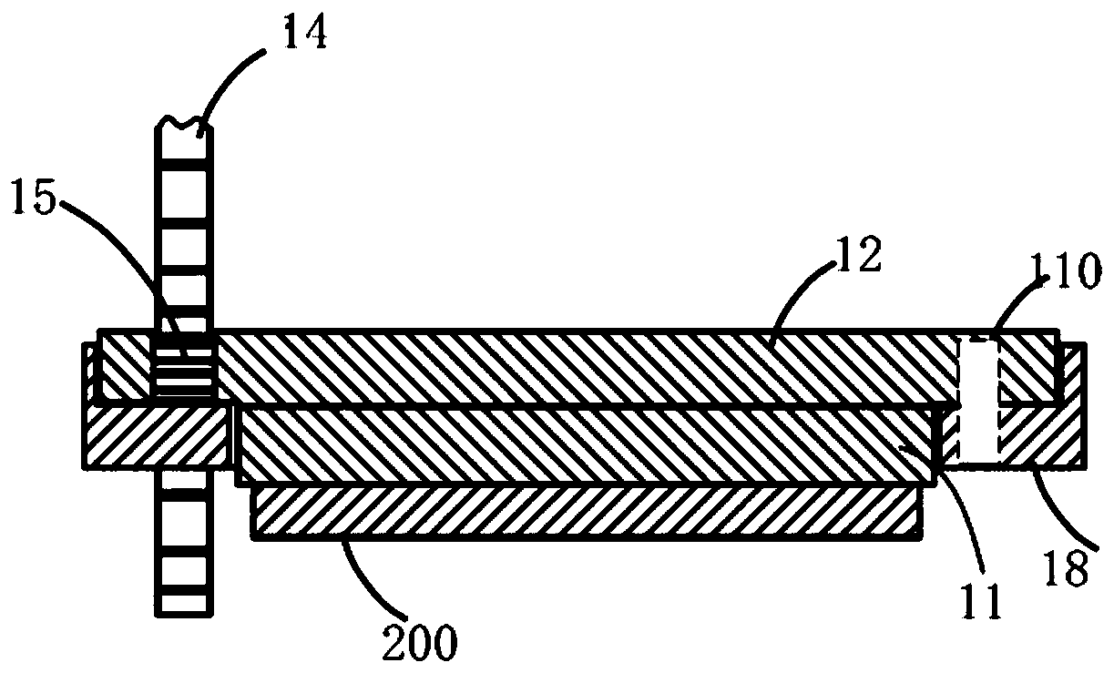
The invention relates to the field of crystal growing of semiconductor materials, and specifically relates to a carbonized silicon single crystal growing device. The device comprises a crucible, a base, an overturning plate and a first driving mechanism, wherein an opening is formed in the top of the crucible, and the crucible is used for storing carbonized silicon raw materials; the surface of one side of the base is a single-crystal growing surface; the overturning plate and the base are arranged at the opening in the top of the crucible; the first driving mechanism is capable of driving thesingle-crystal growing surface of the base through the overturning plate to switch between the state of facing the inside of the crucible and the state of departing from the inside of the crucible. According to the method in the embodiment, a material supplying mechanism is arranged; non-stoichiometric ratio type carbonized silicon rich in carbon is adjusted into non-stoichiometric ratio type carbonized silicon rich in silicon. In addition, the overturning plate is arranged; seed crystals are driven by the overturning plate to depart from the raw materials of the carbonized silicon, so that the problem that the unbalanced carbonized silicon source sublimated to the surface of the seed crystal to cause low crystal quality is avoided. Therefore, the problem that the carbonized silicon changes from rich silicon state to rich carbon state, resulting in reduction of the crystal quality is solved; the crystal growing length is increased; the crystal growing benefit is increased; the carbonized silicon single crystal quality is improved.

Description

technical field [0001] The invention relates to the field of crystal growth of semiconductor materials, in particular to a silicon carbide single crystal growth device and a method for manufacturing a silicon carbide single crystal. Background technique [0002] Silicon carbide, the third-generation semiconductor, is a single crystal grown at high temperature, its hardness is second only to diamond, and its melting point is 2830°C. Difficult growth conditions, resulting in expensive silicon carbide crystal cost. Silicon carbide substrates made of silicon carbide crystals are widely used in electronic power devices and nitride epitaxial growth, and can be widely used in electric vehicles, hybrid vehicles, rail transit, high-frequency devices, microwave devices, etc., with very high economic benefits and national defense value. [0003] It is known from the silicon-carbon binary phase diagram that silicon carbide growth crystals cannot be directly solidified from a single liq...

Claims


Application Information

Patent Timeline
IPC IPC(8): C30B23/00C30B29/36
CPCC30B23/00C30B29/36
Inventor 徐良蓝文安占俊杰阳明益刘建哲余雅俊
Owner 浙江富芯微电子科技有限公司
Learn More