Nitride semiconductor device and method of manufacturing the same

a semiconductor device and nitride technology, applied in the direction of secondary cell servicing/maintenance, non-aqueous electrolyte cells, cell components, etc., can solve the problems of large lattice mismatch to gan of 13%, difficult to maintain the operation reliability of the semiconductor device for a long time, etc., and achieve the effect of increasing the width of the lateral growth region

Inactive Publication Date: 2005-08-25
KOBAYASHI TOSHIMASA +3
View PDF14 Cites 76 Cited by
  • Summary
  • Abstract
  • Description
  • Claims
  • Application Information

AI Technical Summary

Benefits of technology

[0060] The inventors of the present invention focused attention on the fact that in the conventional configurations, the lateral growth of a GaN layer between adjacent seed crystal portions was symmetrically carried out from both sides of the seed crystal portions, and lateral growth regions were met each other at the center between the adjacent seed crystal portions to form a meeting portion, so the inventors had a conception of the invention that the lateral growth of the GaN layer was asymmetrically carried out so as to form the meeting portion in a position away from the center between the adjacent seed crystal portions, thereby the width of the lateral growth region is increased. The conception was confirmed by experiments, and the present invention was achieved.
[0065] In the first nitride semiconductor device according to the invention, the meeting portion is formed in a position away from the center between the adjacent seed crystal portions in a direction parallel to the surface of the substrate, so the width of the lateral growth region is increased with respect to a pitch of the seed crystal portion (the sum of the width of the seed crystal portion and the width of a region between the adjacent seed crystal portions), that is, the value of (the width of the lateral growth region) / (the pitch of the seed crystal portion) is large.
[0066] In the second nitride semiconductor device according to the invention, the meeting portion is formed in a position away from the center between the adjacent seed crystal portions in a direction parallel to the surface of the substrate, so the width of the lateral growth region is increased with respect to a pitch of the mask (the sum of the width of the mask and the width of a region between the adjacent masks), that is, the value of (the width of the lateral growth region) / (the pitch of the mask) is large.

Problems solved by technology

A problem which arises when a semiconductor device with high reliability is made by the use of the nitride compound semiconductors is that there is no suitable substrate material.
In other words, in obtaining a high-quality nitride compound semiconductor layer, the following problems with the nitride compound semiconductors and the substrate material arise.
While the sapphire substrate has an advantage in production control that high-quality 2-inch substrates or 3-inch substrates are stably supplied to markets, it has a technical disadvantage of a large lattice mismatch to GaN of 13%.
Therefore, it is difficult to maintain the operational reliability of the semiconductor device for a long time.
Moreover, the sapphire substrate has the following problems: (1) the sapphire substrate has no cleavage, so it is difficult to stably form a laser facet with high mirror reflectance, (2) sapphire is an insulator, so it is difficult to dispose an electrode on the back side of the substrate as in the case of a GaAs semiconductor laser device, and both of a p-side electrode and an n-side electrode must be disposed on the side of a laminate of the nitride compound semiconductor layers on the substrate, and (3) there is a large difference in the thermal expansion coefficient between the sapphire substrate and the GaN layer, so there are a number of restrictions in a process of forming the device, for example, that when a crystal growth film is thick, a large warp in the substrate occurs even at room temperature, and thereby a crack may occur.
However, defects or the like in the meeting portion still remain, so a high-quality GaN layer cannot be formed all over the substrate.
Thus, even in the first through the fourth examples and combinations of the examples, it is difficult to obtain a substrate with a low defect density as a whole.
It is considered that when the thickness of a crystal growth film including a device portion such as the semiconductor laser device is nearly equal to the cycle of the crystal portion or the mask, a defect distribution during growth in a substantially lateral direction is reflected to the uppermost surface of a laminate including the device portion, so crystal defects occur in the device portion.
However, in fact, as shown in FIG. 13B or 14B, the GaN layer 15 is formed through laterally growing GaN crystals from both side surfaces of the seed crystal portion 11, so in the meeting portion 32, the crystals are not fully matched, thereby resulting in the occurrence of defects.
In the above description, although problems are described referring to the GaN layer as an example, they are universal problems when a laminate of the nitride compound semiconductor layers is formed.

Method used


Image

  • Nitride semiconductor device and method of manufacturing the same
  • Nitride semiconductor device and method of manufacturing the same
  • Nitride semiconductor device and method of manufacturing the same

Examples


first embodiment

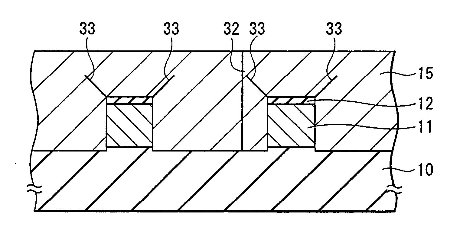
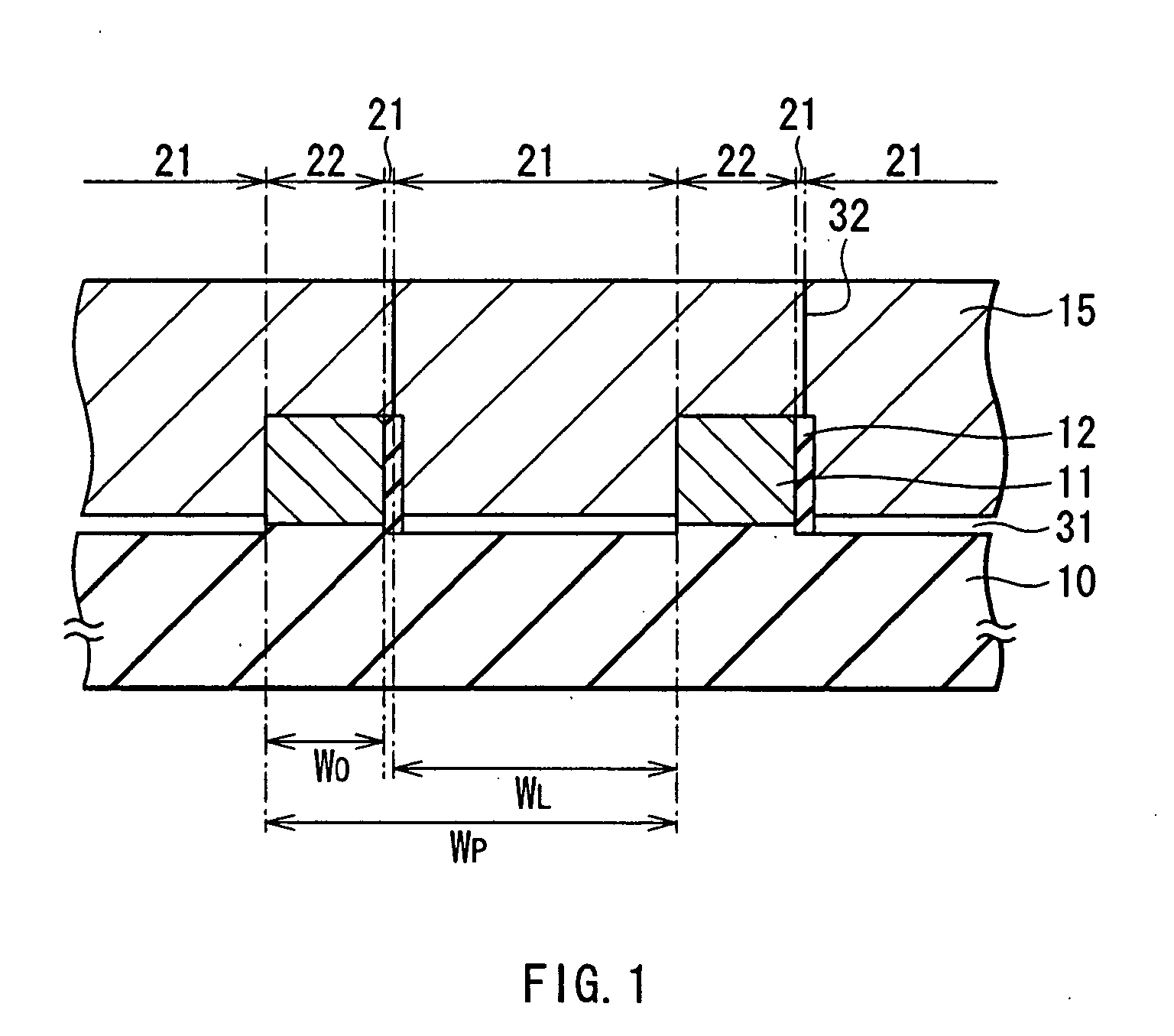
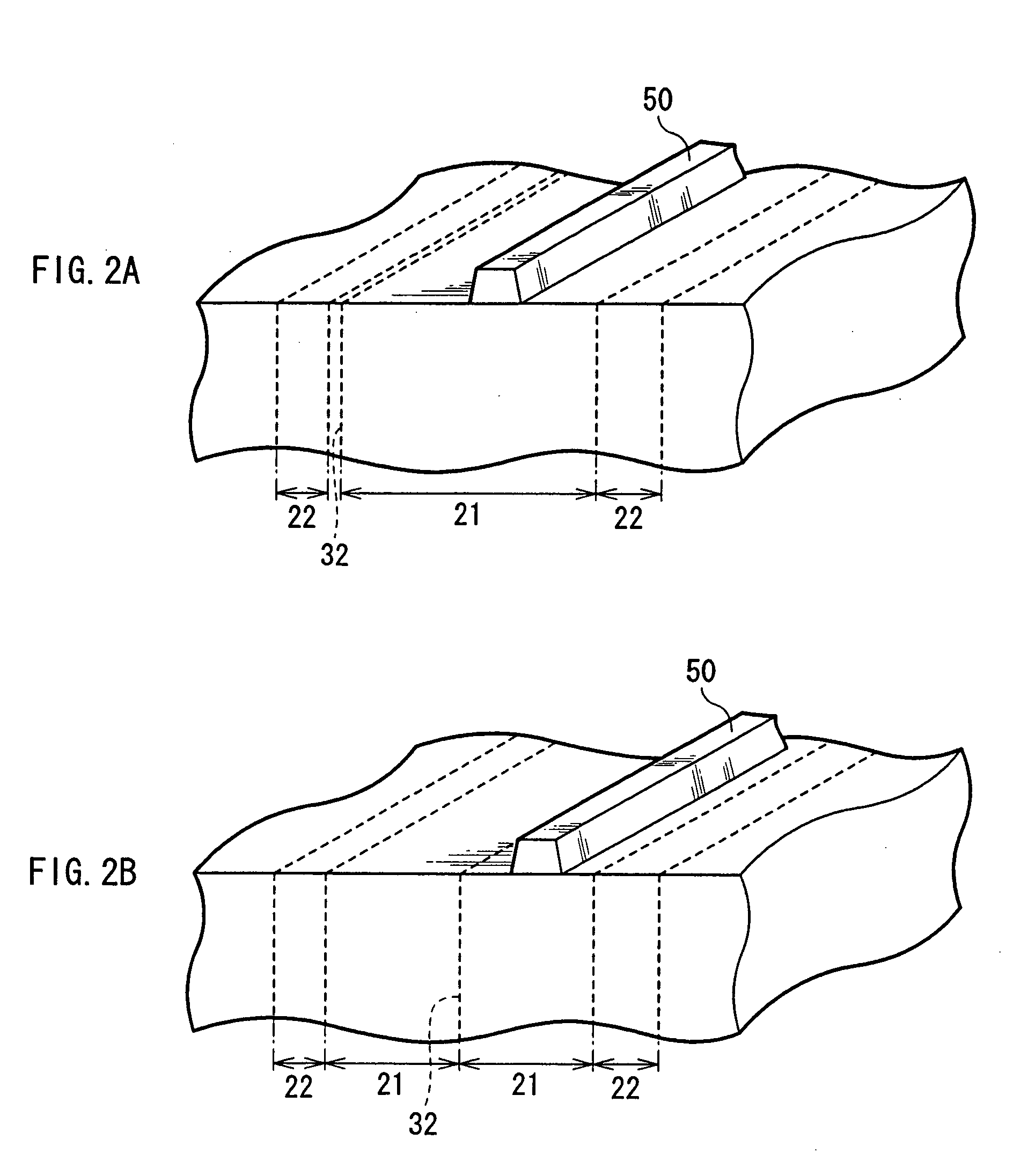
[0089]FIG. 1 shows a configuration of main components of a nitride semiconductor device according to a first embodiment of the invention.

[0090] As shown in FIG. 1, the nitride semiconductor device mainly comprises a plurality of seed crystal portions 11 each of which is formed in a stripe shape on a sapphire substrate 10 and has a mask 12 on one side surface, and a GaN layer 15 which is a crystal layer grown on the sapphire substrate 10 and the seed crystal portions 11 through epitaxial lateral overgrowth.

[0091] In the configuration, the GaN layer 15 is grown only from an exposed side surface of the seed crystal portion 11 which is not covered with the mask 12, so the lateral growth of the GaN layer 15 is asymmetrically carried out, thereby a meeting portion 32 is formed in the vicinity of a boundary between the seed crystal portion 11 and the mask 12 in a thickness direction (laminated direction) of the GaN layer 15.

[0092] In conventional configurations, for example, as shown in...

second embodiment

[0103]FIG. 4B shows a configuration of main components of a nitride semiconductor device according to a second embodiment of the invention.

[0104] As shown in FIG. 4B, the nitride semiconductor device improves the conventional nitride semiconductor device in the first example, and the nitride semiconductor device comprises the mask 12 which is disposed on the seed crystal layer 11A and has an end 12a with a larger thickness than other portions, and the GaN layer 15 which is a crystal layer grown on the seed crystal layer 11A through the epitaxial lateral overgrowth so as to cover the mask 12.

[0105] In the nitride semiconductor device, a time difference in the start of the lateral growth of the GaN layer 15 occurs because of the difference in the thickness of the mask 12, so the lateral growth is carried out asymmetrically with respect to the mask 12. As a result, the meeting portion 32 is formed not in the center of the mask 12 like the first example, but in a position in the vicin...

third embodiment

[0112]FIG. 5 shows a configuration of main components of a nitride semiconductor device according to a third embodiment of the invention.

[0113] The nitride semiconductor device comprises a plurality of seed crystal portions 11 each of which is formed on the sapphire substrate 10 and has the mask 12 on the top surface and one side surface, and the GaN layer 15 which is a crystal layer grown on the sapphire substrate 10 and the seed crystal portions 11 through the epitaxial lateral overgrowth.

[0114] The lateral growth of the GaN layer 15 is carried out only from an exposed surface of the seed crystal portion 11 which is not covered with the mask 12, so the growth is asymmetric, and as shown in FIG. 5, the meeting portion 32 is formed in the vicinity of the boundary between the seed crystal portion 11 and the mask 12 disposed on the side surface of the seed crystal portion 11 in the thickness direction of the GaN layer 15.

[0115] In the embodiment, the meeting portion 32 is formed in...


PUM

PropertyMeasurementUnit
crystal growth temperatureaaaaaaaaaa
widthaaaaaaaaaa
widthaaaaaaaaaa

Abstract

Provided is a nitride semiconductor device with high reliability and high flexibility in design and manufacture of the device. The nitride semiconductor device comprises a seed crystal portion (11) formed on a sapphire substrate (10) and having a mask (12) on one side surface thereof, and a GaN layer (15) grown on the sapphire substrate (10) and the seed crystal portion (11) through epitaxial lateral overgrowth. The GaN layer (15) is grown only from an exposed side surface of the seed crystal portion (11) which is not covered with the mask (12), so the lateral growth of the GaN layer (15) is asymmetrically carried out. Thereby, a meeting portion (32) is formed in the vicinity of a boundary between the seed crystal portion (11) and the mask (12) in a thickness direction of the GaN layer (15). Therefore, as the meeting portion (32) is formed in a position away from the center between the adjacent seed crystal portions (11) in a direction parallel to a surface of the substrate, a width WL of a lateral growth region is larger with respect to a pitch WP of the seed crystal potion (11), compared with conventional configurations.

Description

TECHNICAL FIELD [0001] The present invention relates to a nitride semiconductor device comprising a nitride compound semiconductor layer on a substrate and a method of manufacturing the same. BACKGROUND ART [0002] Characteristics of Group III nitride compound semiconductors (hereinafter referred to as nitride compound semiconductors) such as GaN, AlGaN, GaInN, AlGaInN and AlBGaInN include that they have a larger band gap energy Eg than Group III-V compound semiconductors such as AlGaInAs and AlGaInP, and they are direct transition semiconductors. [0003] Because of the characteristics, attention has been given to the nitride compound semiconductors as materials of semiconductor light emitting devices such as semiconductor laser devices which emit light in a short wavelength range from ultraviolet to green and light emitting diodes (LEDs) capable of emitting light in a wider wavelength range from ultraviolet to red. [0004] These semiconductor light emitting devices are being widely ap...

Claims


Application Information

Patent Timeline
Patent Type & Authority Applications(United States)
IPC IPC(8): H01L21/20H01L21/336H01L29/20H01L33/00H01M2/02H01M4/02H01M4/48H01M4/52H01M4/62H01M6/10H01M6/16H01M10/40H01M10/42
CPCC30B25/04C30B29/403H01L21/0242H01L21/0254H01L33/007H01L21/02647H01L21/0265H01L29/2003H01L29/66522H01L21/02639
Inventor KOBAYASHI, TOSHIMASAYANASHIMA, KATSUNORIYAMAGUCHI, TAKASHINAKAJIMA, HIROSHI
Owner KOBAYASHI TOSHIMASA
Why Eureka
Try Eureka