Method and apparatus for manufacturing group iii nitride crystals

a technology of nitride crystals and manufacturing methods, applied in the direction of crystal growth process, polycrystalline material growth, crystal growth process, etc., can solve the problems of high pressure resistance characteristic deterioration, low defect density, and complicated apparatus, etc., to achieve the effect of low defect density

Inactive Publication Date: 2007-09-20
NGK INSULATORS LTD
View PDF24 Cites 77 Cited by
  • Summary
  • Abstract
  • Description
  • Claims
  • Application Information

AI Technical Summary

Benefits of technology

[0066]According to the present invention, it is possible to obtain a material which is a GaN substrate having such low defect density that can be used as a power semiconductor substrate, and in which n-type and p-type characteristics required for formation of a transistor or the like are controlled. Further, it is possible to massively produce bulk GaN substrates having diameter required for a power semiconductor substrate of 3 inches or more, preferably 5 inches or more.

Problems solved by technology

Although various growth methods of semiconductor laser substrate have been conventionally studied as for the GaN substrate which forms a base, those having such low defect density that allows use as a power semiconductor substrate have not been obtained.
However, the above substrate is not satisfactory as a bulk GaN substrate for power semiconductor for which low defect density of not more than 104 per square centimeter is required over the entire area of several millimeters square, and thus leads the problem of deterioration in high pressure resistance characteristic due to such defect.
During this time, a mechanism for evaporating and solidifying Na or additionally charging Ga or additive elements for growing ingot from uniform flux composition is required, and the seed crystal position should be precisely controlled by scanning the growth condition, which complicate the apparatus.

Method used


Image

  • Method and apparatus for manufacturing group iii nitride crystals
  • Method and apparatus for manufacturing group iii nitride crystals
  • Method and apparatus for manufacturing group iii nitride crystals

Examples


example 1

[0080]Next, a method of producing a plurality of silicon doped bulk GaN substrates which may be used as n-type semiconductor substrates will be explained.

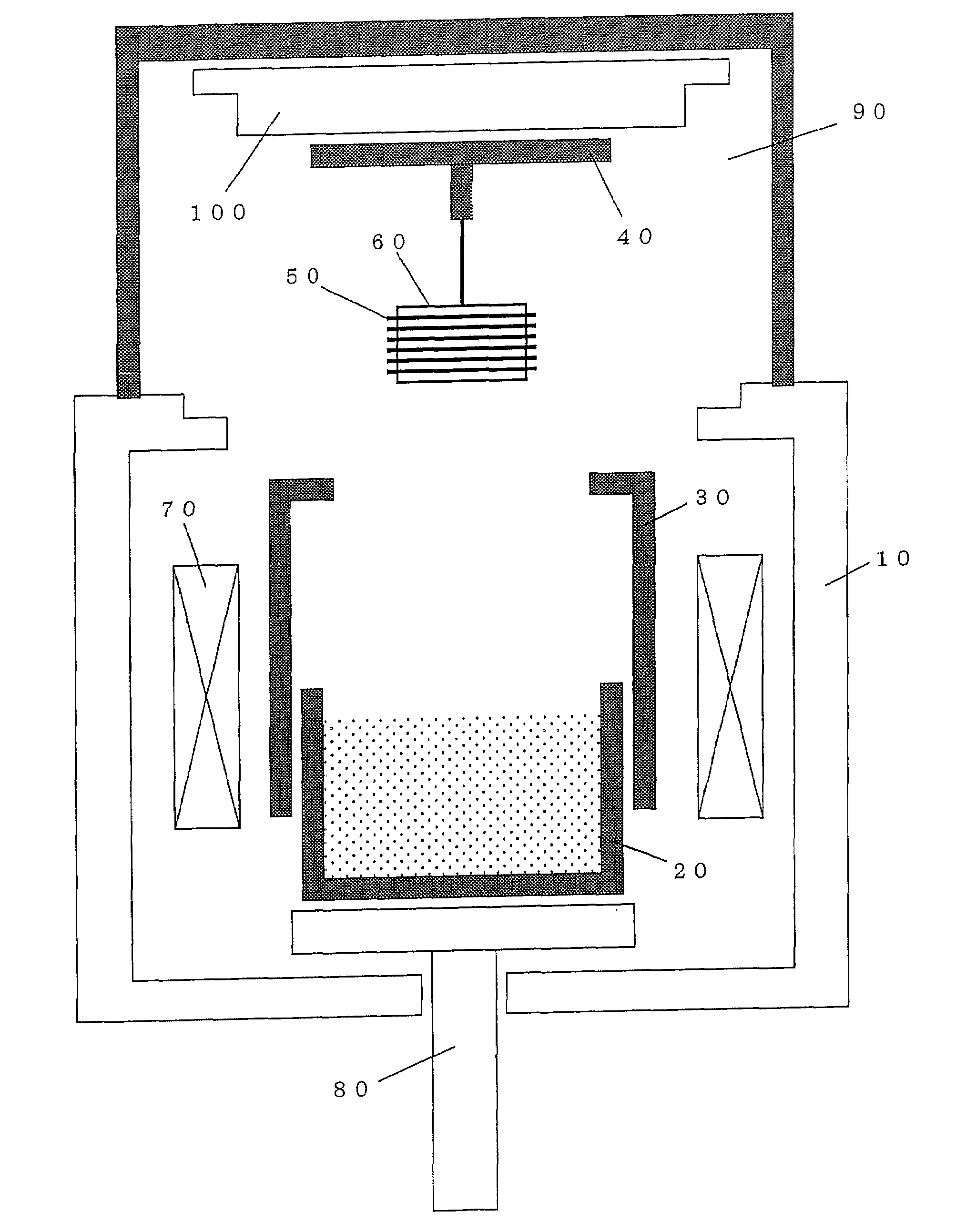
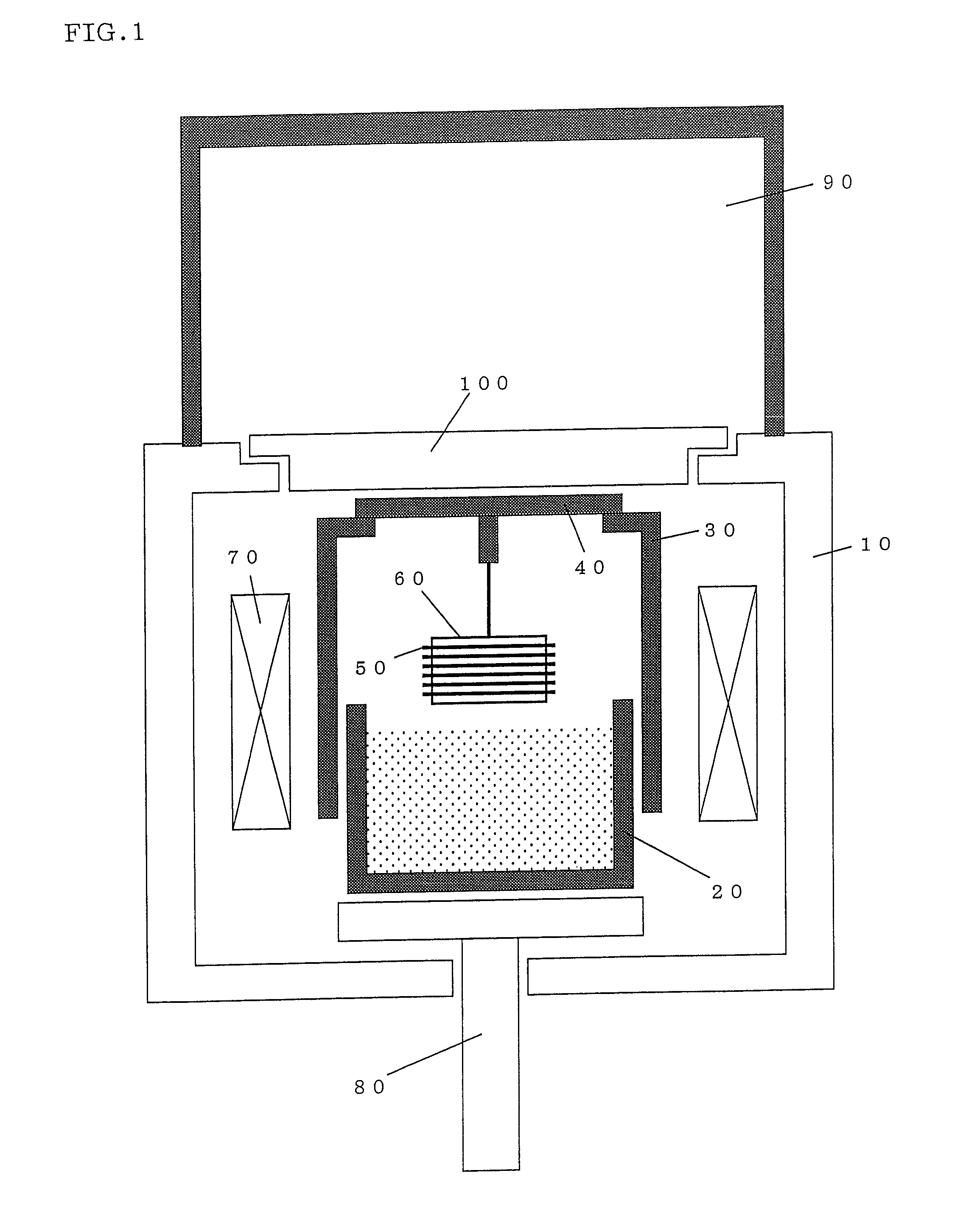
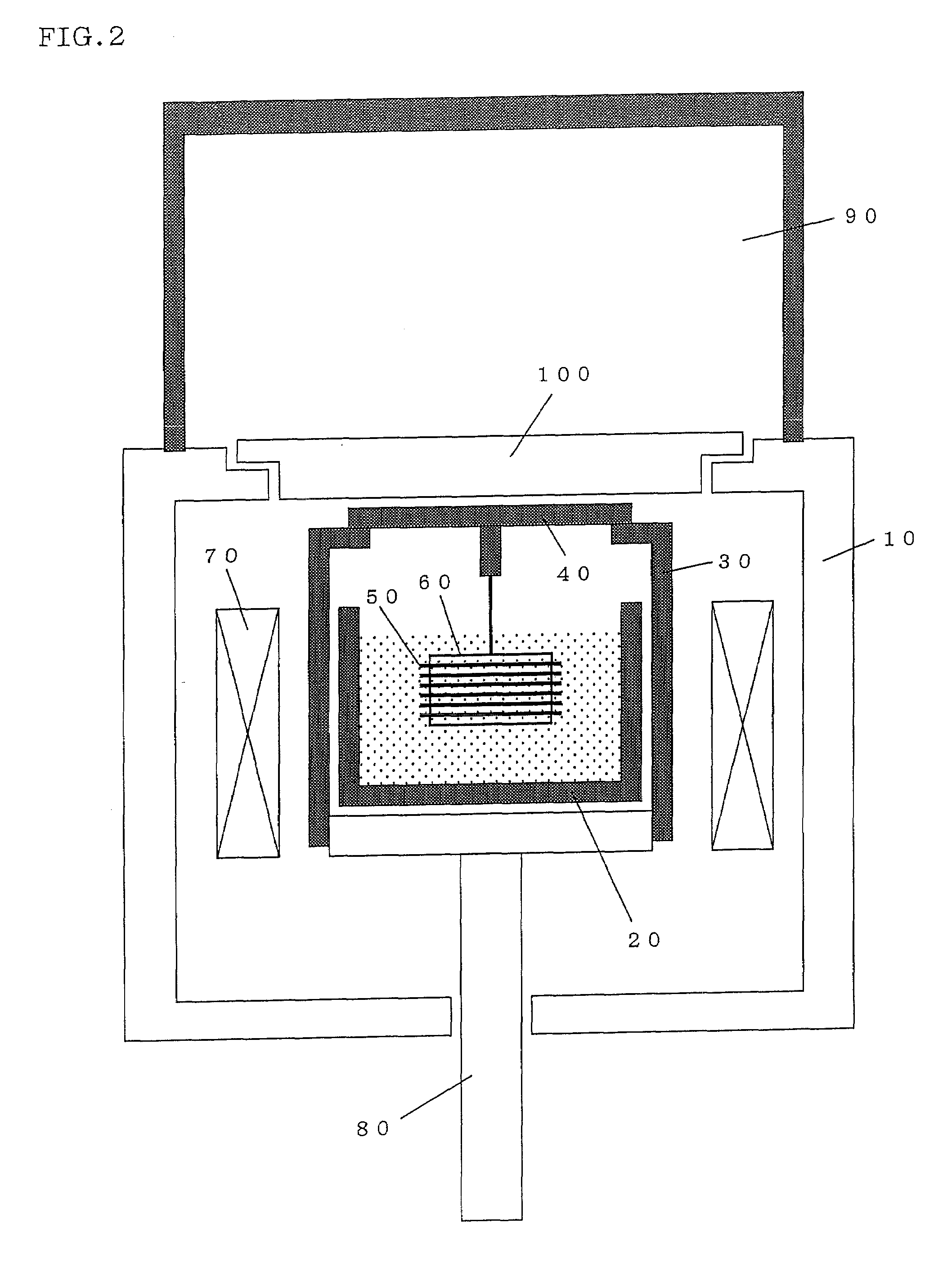
[0081]In the state of FIG. 3, using a metal tantalum crucible having an inner diameter of 150 mm, and a thickness of 2 mm as the reaction vessel 20, about 2000 grams of metal Na, about 2000 grams of metal Ga and a required amount of metal Si were charged.

[0082]As the seed crystal substrate 50, fifty substrates were prepared each obtained by causing 400 nm of GaN thin film to grow by MOCVD method on a sapphire C face substrate having a diameter of 100 mm and a thickness of 500 μm, vapor depositing 20 nm of titanium metal thin film, heating for several tens minutes at about 1000° C. with mixed gas of hydrogen and argon, and causing about 2 μm of GaN thin film to grow by MOCVD method.

[0083]These fifty seed crystal substrates were arranged substantially horizontally in the arrangement member 60 at 2 mm interval, and placed below the up...

example 2

[0091]Next, a method of producing a plurality of magnesium doped bulk GaN substrates which may be used as a p-type semiconductor substrate will be explained. Structure of the apparatus is as same as that described above.

[0092]Using as the reaction vessel 20, a metal tantalum crucible having an inner diameter of 150 mm and a thickness of 2 mm, about 2000 grams of metal Na, about 2000 grams of metal Ga and a required amount of metal Mg were charged.

[0093]As the seed crystal substrate 50, fifty substrates were prepared each obtained by causing 400 nm of GaN thin film to grow by MOCVD method on a sapphire C face substrate having a diameter of 100 mm and a thickness of 500 μm, forming a stripe silicon oxide mask pattern thin film of about 10 μm by line&space, and causing about 20 μm of GaN thin film to grow by HVPE method.

[0094]Growth experiment was conducted in the same condition as in Example 1, and the grown single-crystal GaN wafer was taken out as a self-standing substrate peeled fr...

example 3

[0097]Next, a method of making the plurality of GaN substrate surface grown at high speed by HVPE method into a silicon-doped GaN substrates which may be used as an n-type semiconductor will be explained. Structure of the apparatus is similar to the above structure.

[0098]Using as the reaction vessel 20, a metal tantalum crucible having an inner diameter of 150 mm and a thickness of 2 mm, about 2300 grams of metal Na, about 500 grams of metal Ga and a required amount of metal Si were charged.

[0099]As the seed crystal substrate 50, fifty wafers of 500 μm thick obtained through cutting process and polishing process after growing a C face GaN substrate having a diameter of 100 mm and a thickness of 50 mm by HVPE method were used. In setting, the substrates were set so that the Ga face (+face) which is to be a growth face was downside.

[0100]Growth experiment was conducted in the same condition as in Example 1 except that the growth time was 5 hours, and the grown single-crystal GaN wafer...


PUM

PropertyMeasurementUnit
thicknessaaaaaaaaaa
thicknessaaaaaaaaaa
temperatureaaaaaaaaaa

Abstract

There is provided a group III nitride crystal growth method capable of obtaining a material which is a GaN substrate of low defect density capable of being used as a power semiconductor substrate and in which characteristics of n-type and p-type requested for formation of transistor or the like. A growth method of group III nitride crystals includes: forming a mixed melt containing at least group III element and a flux formed of at least one selected from the group consisting of-alkaline metal and alkaline earth metal, in a reaction vessel; and growing group III nitride crystals from the mixed melt and a substance containing at least nitrogen, wherein after immersing a plurality of seed crystal substrates placed in an upper part of the reaction vessel in which the mixed melt is formed, into the mixed melt to cause crystal growth, the plurality of seed crystal substrates are pulled up above the mixed melt.

Description

BACKGROUND OF THE INVENTION AND RELATED ART STATEMENT[0001]The present invention relates to a method and apparatus for manufacturing a group III nitride substrate.[0002]Group III nitride semiconductors such as gallium nitride (GaN) are expected for application to a power semiconductor, namely a semiconductor device controlling large electric current, and is requested to have high forward blocking voltage, high current multiplication rate and stable or positive thermal coefficient over existent silicon-based semiconductors.[0003]It is known that a power controlling device such as inverter having higher efficiency and smaller size than a silicon-based semiconductor can be realized when such a semiconductor device as described above is realized and used in a hybrid automobile or power supply / distribution facility. In particular, a great merit is provided that a cooling-related mechanism of a power semiconductor can be dispensed with. Development using SiC-based material as a substrate ...

Claims


Application Information

Patent Timeline
Patent Type & Authority Applications(United States)
IPC IPC(8): C30B15/00C30B21/06
CPCC30B9/10C30B19/02Y10T117/1032C30B7/00C30B29/403
Inventor IMAEDA, MINORUKONDO, YOSHIMASAOKAZAKI, ICHIRO
Owner NGK INSULATORS LTD
Why Eureka
Try Eureka